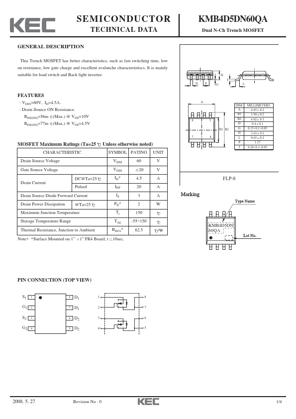
KMB4D5DN60QA Description
This Trench MOSFET has better characteristics, such as fast switching time, low on resistance, low gate charge and excellent avalanche characteristiscs. It is mainly suitable for load switch and Back light inverter.
KMB4D5DN60QA Key Features
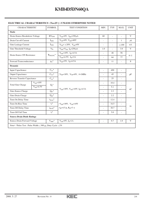
- 100 nA
- 46 56 m
- pF nC ns
- 0.7 1.0
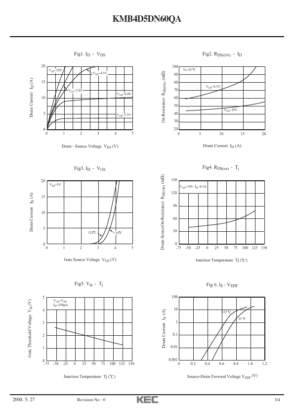
- Source Voltage VDS (V)