KML0D4N20V Description
It s mainly suitable for Load Switching Cell Phones, Battery Powered Systems and Level-Shifter.
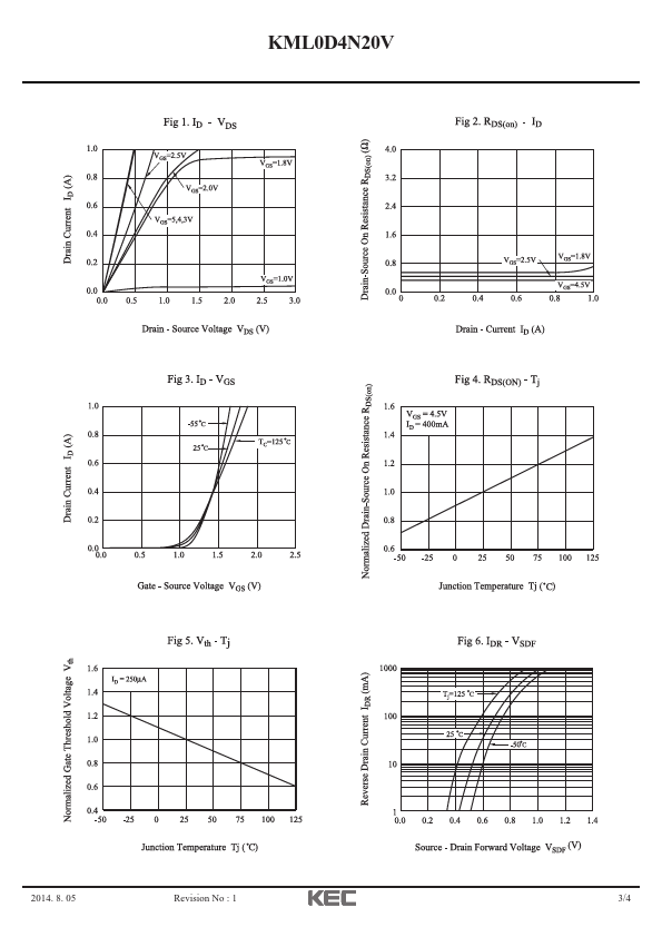
KML0D4N20V Key Features
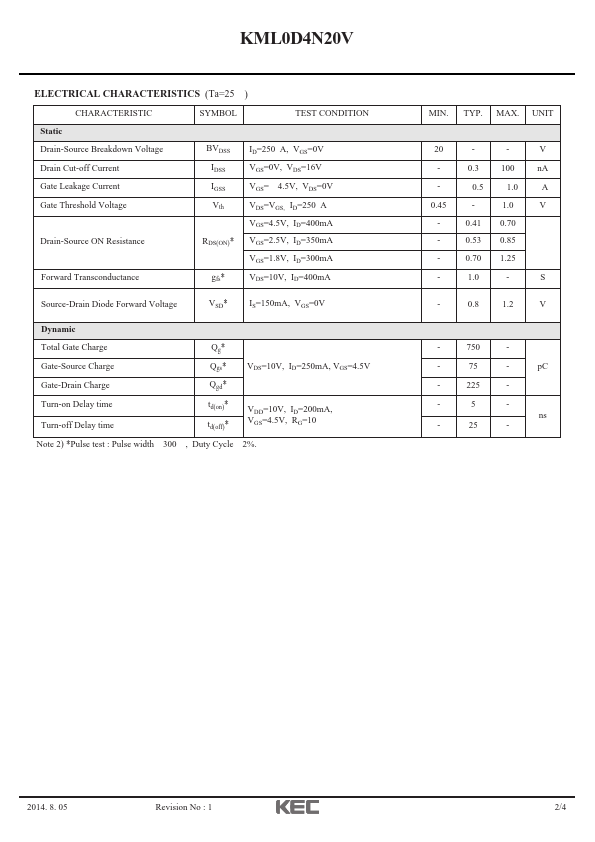
- 0.3 100 nA
- 0.5 1.0 A
- 0.41 0.70
- 0.53 0.85
- 0.70 1.25
- 0.8 1.2 V
- 225 -5- 25
KML0D4N20V is N-Channel MOSFET manufactured by KEC.
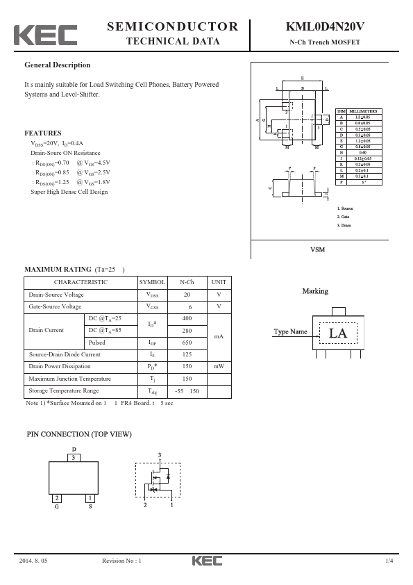
It s mainly suitable for Load Switching Cell Phones, Battery Powered Systems and Level-Shifter.