FEATURES
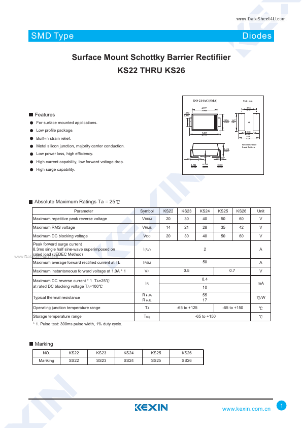
For surface mounted applications. Low profile package. Built-in strain relief. Metal silicon junction, majority carrier conduction. Low power loss, high efficiency. High current capability, low forward voltage drop. High surge capability. 1.575 1.397 2 1 2.896 2.489 1.67 1.47 5.283 4.775 2.38 2.18 5.49 5.29 Recommended Land Pattern 2.438 1.981 1.524 0.762 0.203 0.051 0.305 0.152 ABSOLUTE MAXIMUM RATINGS
Ta = 25 Parameter Maximum repetitive peak reverse voltage Maximum RMS voltage Maximum DC blocking voltage Peak forward surge current 8.3ms single half sine-wave superimposed on rated load (JEDEC Method) Maximum average forward rectified current at TL Maximum instantaneous forward voltage at 1.0A * 1 Maximum DC reverse current * 1 TA=25 at rated DC blocking voltage TA=100 Typical thermal resistance Operating junction temperature range Storage temperature range * 1. Pulse test: 300ms pulse width, 1% duty cycle. Symbol VRRM VRMS VDC I(AV) IFSM VF IR 10 R R JA JL KS22 20 14 20 KS23...