KNX7150A
Features n Proprietary New Planar Technology n RDS(ON),typ.=0.24Ω@VGS=10V n Low Gate Charge Minimize Switching Loss n Fast Recovery Body Diode
2.Applications n Adaptor Charger n SMPS Power Supply n LCD Panel Power
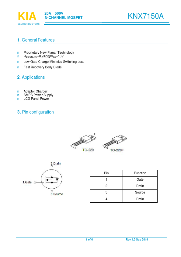
3. Pin configuration
Pin
Function
Gate
Drain
Source
Drain
1 of 6
Rev 1.0 Sep 2019
SEMICONDUCTORS
20A,500V N-CHANNEL MOSFET
4. Ordering Information
Part Number
KNP7150A KNF7150A
Package
TO-220 TO-220F
Brand
KIA KIA
5. Absolute maximum ratings
Symbol
Parameter
VDSS VGSS
IDM EAS dv /dt
TL TPAK TJ&TSTG
Drain-to-Source Voltage[1]
Gate-to-Source Voltage
Continuous Drain Current Continuous Drain Current@ Tc=100 ºC Pulsed Drain Current at VGS=10V[2]
Single Pulse Avalanche Energy Peak Diode Recovery dv/dt[3]
Power Dissipation Derating Factor above 25 ºC Maximum Temperature for Soldering Leads at 0.063in (1.6mm) from Case for 10 seconds, Package Body for 10 seconds Operating and Storage Temperature Range
(TC= 25 ºC , unless...