KK4502B
KK4502B is Strobed Hex Inverter/Buffer High-Voltage Silicon-Gate CMOS manufactured by Kodenshi AUK Group.
..
TECHNICAL DATA
Strobed Hex Inverter/Buffer
High-Voltage Silicon-Gate CMOS
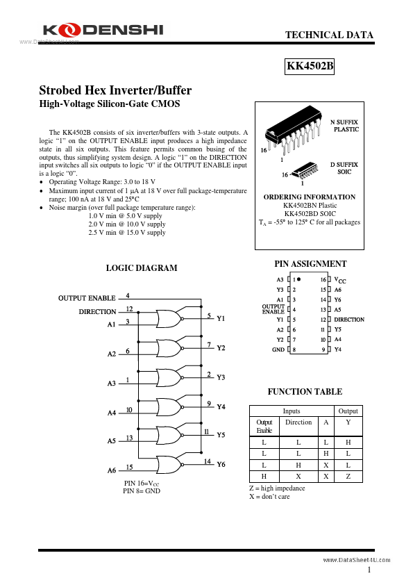
The KK4502B consists of six inverter/buffers with 3-state outputs. A logic “1” on the OUTPUT ENABLE input produces a high impedance state in all six outputs. This feature permits mon busing of the outputs, thus simplifying system design. A logic “1” on the DIRECTION input switches all six outputs to logic “0” if the OUTPUT ENABLE input is a logic “0”.
- Operating Voltage Range: 3.0 to 18 V
- Maximum input current of 1 µA at 18 V over full package-temperature range; 100 nA at 18 V and 25°C
- Noise margin (over full package temperature range): 1.0 V min @ 5.0 V supply 2.0 V min @ 10.0...