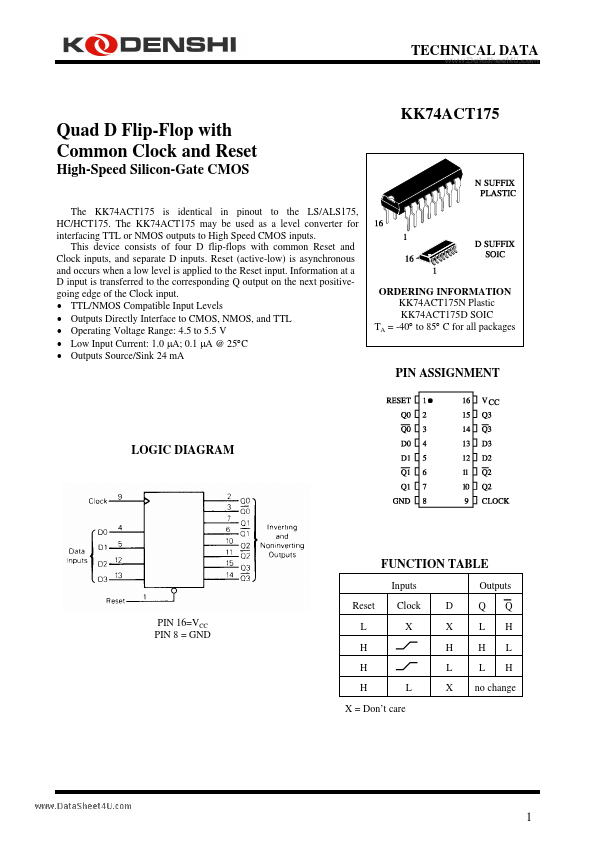
KK74ACT175
TECHNICAL DATA
..
Quad D Flip-Flop with mon Clock and Reset
High-Speed Silicon-Gate CMOS
The KK74ACT175 is identical in pinout to the LS/ALS175, HC/HCT175. The KK74ACT175 may be used as a level converter for interfacing TTL or NMOS outputs to High Speed CMOS inputs. This device consists of four D flip-flops with mon Reset and Clock inputs, and separate D inputs. Reset (active-low) is asynchronous and occurs when a low level is applied to the Reset input. Information at a D input is transferred to the corresponding Q output on the next positivegoing edge of the Clock input.
- TTL/NMOS patible Input Levels
- Outputs Directly Interface to CMOS, NMOS, and TTL
- Operating Voltage Range: 4.5 to 5.5 V
- Low Input Current: 1.0 µA; 0.1 µA @ 25°C
- Outputs Source/Sink 24 m A
ORDERING INFORMATION KK74ACT175N Plastic KK74ACT175D SOIC TA = -40° to 85° C for all packages
PIN ASSIGNMENT
LOGIC DIAGRAM
FUNCTION TABLE
Inputs Reset PIN 16=VCC PIN 8 = GND L H H H X = Don’t care L Clock X...