KK74HC651A
KK74HC651A is Octal 3-State Bus Transceivers and D Flip-Flops manufactured by Kodenshi AUK Group.
TECHNICAL DATA
Octal 3-State Bus Transceivers and D Flip-Flops
High-Performance Silicon-Gate CMOS
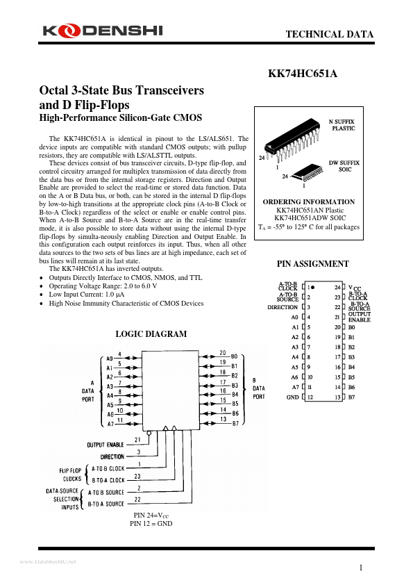
The KK74HC651A is identical in pinout to the LS/ALS651. The device inputs are patible with standard CMOS outputs; with pullup resistors, they are patible with LS/ALSTTL outputs. These devices consist of bus transceiver circuits, D-type flip-flop, and control circuitry arranged for multiplex transmission of data directly from the data bus or from the internal storage registers. Direction and Output Enable are provided to select the read-time or stored data function. Data on the A or B Data bus, or both, can be stored in the internal D flip-flops by low-to-high transitions at the appropriate clock pins (A-to-B Clock or B-to-A Clock) regardless of the select or enable or enable control pins. When A-to-B Source and B-to-A Source are in the real-time transfer mode, it is also possible to store data without using the internal D-type flip-flops by simulta-neously enabling Direction and Output Enable. In this configuration each output reinforces its input. Thus, when all other data sources to the two sets of bus lines are at high impedance, each set of bus lines will remain at its last state. The KK74HC651A has inverted outputs.
- Outputs Directly Interface to CMOS, NMOS, and TTL
- Operating Voltage Range: 2.0 to 6.0 V
- Low Input Current: 1.0 µA
- High Noise Immunity Characteristic of CMOS Devices
ORDERING INFORMATION KK74HC651AN Plastic KK74HC651ADW SOIC TA = -55° to 125° C for all packages
PIN ASSIGNMENT
LOGIC DIAGRAM
PIN 24=VCC PIN 12 = GND
..net
MAXIMUM RATINGS-
Symbol VCC VIN VOUT IIN IOUT ICC PD Tstg TL
- Parameter DC Supply Voltage (Referenced to GND) DC Input Voltage (Referenced to GND) DC Output Voltage (Referenced to GND) DC Input Current, per Pin DC Output Current, per Pin DC Supply Current, VCC and GND Pins Power Dissipation in Still Air, Plastic DIP+ SOIC Package+ Storage Temperature Lead Temperature, 1 mm...