KKA2586
KKA2586 is 1024 x 8-Bit n-MOS EEPROM manufactured by Kodenshi AUK Group.
FEATURES
- -
- -
- -
- -
- Non-volatile storage of information during 10 years Single supply (Ucc=4,75 B
- 5,25 B) On-chip voltage multiplier On-chip generator of bulk biasing Serial input/output I2C-bus 10 000 ERASE/WRITE cycles per byte; Internal reprogramming (no external ponents) Duration of the ERASE/WRITE cycle is 15 ms Temperature range: 0 ÷ +700C
ELECTRICAL CHARACTERISTICS
Parameter Supply current, m A Output low voltage (SDA), V High leakage current: -on output (SDA), µA -on inputs SCL, SDA, µA -on inputs CS, TP1, TP2,µA Input capacitance, p F Clock input frequency, k Hz Reprogramming cycle time, ms Erase of die cycle time, ms The number of E/W cycles on 1 byte Input high voltage: -inputs SDA, SCL, V -inputs CS, TP1, TP2, V Input low voltage: -inputs SDA, SCL, V -inputs CS, TP1, TP2, V Conditions UCC=5.25 B IOL=3 m A UCC=4.75B UOH=5,25 B UIH=5,25 B UIH=5,25 B UI= 0 B Erase and Write UTP2= 5,0 B Symbol ICC0 UOL Min. Max 20,0 0,4
ILOH ILIH ILIH CI f SCL t PROG t ER
0 10,0 10 000 3,0 4,5
- 10,0 10,0 100,0 10,0 100 20,0 20,0 UCC UCC 1,5 0,2 KK
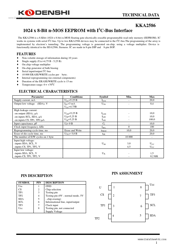
PIN DESCRIPTION
SYMBOL Uss CS TP1 TP2 SDA SCL TP3 Ucc PIN 1 2 3 4 5 6 7 8 DESCRIPTION
GND Chip selection Testing pin Testing pin (0V
- normal mode, 5V
- chip erasing) Informational line, input/output Clock input Testing pin, not connected Supply Voltage
PIN ASSIGNMENT
Ucc TP3
U CS
1 2
8 7
TP1
3 4
6 5
TP2
..
N SUFFIX PLASTIC DIP (MS
- 001BA)
A 8 5 B 1 4
Dimension, mm Symbol A B MIN 8.51 6.1 MAX 10.16 7.11 5.33 0.36 1.14 2.54 7.62 0° 2.92 7.62 0.2 0.38 10° 3.81 8.26 0.36 0.56 1.78
C -T-...