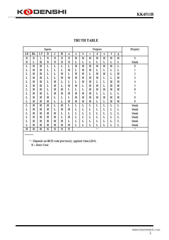
Kodenshi AUK Group KK4511B
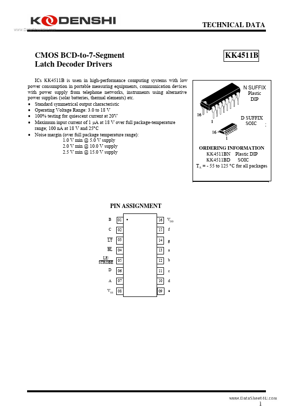
KK4511B is usen in high-performance computing systems with low power consumption in portable measuring equipments, communication devices with power supply from telephone networks, instruments using alternative power supplies (solar batteries, thermal elements) etc.| Part No. | KK4511B |
|---|---|
| Datasheet | KK4511B Download |
| Manufacturer |  Kodenshi AUK Group |
| Description | CMOS BCD-to-7-Segment Latch Decoder Drivers |
| Buy | Stock & Price |
MAXIMUM RATINGS
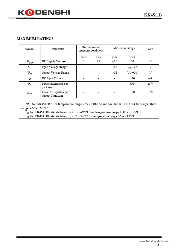
Symbol Parameter Recommended operating conditions min 3 max 18 Maximum ratings min -0.5 -0.5 -0.5 max 20 VDD+0.5 VDD+0.5 ±10 500* 100 Unit VDD VI VO II PD Ptot DC Supply Voltage Input Voltage Range Output Voltage Range DC Input Current Power dissipation per package Power Dissipation per Output Transistor V V V mА mW mW *PD for KK4511BN for temperature range - 55 - +100 °С and for ICs KK4511BD for temperature range - 55 - +65 °С PD for KK4511BN derate linearity at 12 mW/°C for temperature range +100 - +125°C. PD for KK4511BD derate linearity at 7 mW/°C for temperature range +65- +125°C. 3 KK4511B STATIC ELECTRICAL CHARACTERISTIC VDD, Symbol Parameter Test conditions V -55°C min VIH Minimum High- VO = 0.5 V or VDD-1.2 V Level Input VO = 1.0 V or VDD-1.2 V Voltage VO = 1.5 V or VDD-1.2 V Maximum Low VO = 0.5 V or VDD-1.2 V -Level Input VO = 1.0 V or VDD-1.2 V Voltage VO = 1.5 V or VDD-1.2 V High-Level VI = VSS or VDD Output Voltage Low-Level VI = VSS or VDD Output Voltage...