MAXIMUM RATINGS
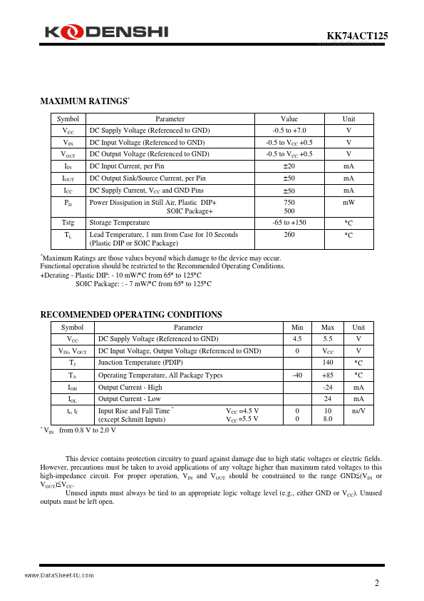
* Symbol VCC VIN VOUT IIN IOUT ICC PD Tstg TL * Parameter DC Supply Voltage (Referenced to GND) DC Input Voltage (Referenced to GND) DC Output Voltage (Referenced to GND) DC Input Current, per Pin DC Output Sink/Source Current, per Pin DC Supply Current, VCC and GND Pins Power Dissipation in Still Air, Plastic DIP+ SOIC Package+ Storage Temperature Lead Temperature, 1 mm from Case for 10 Seconds (Plastic DIP or SOIC Package) Value -0.5 to +7.0 -0.5 to VCC +0.5 -0.5 to VCC +0.5 ±20 ±50 ±50 750 500 -65 to +150 260 Unit V V V mA mA mA mW °C °C MAXIMUM RATINGS
are those values beyond which damage to the device may occur. Functional operation should be restricted to the Recommended Operating Conditions. +Derating - Plastic DIP: - 10 mW/°C from 65° to 125°C SOIC Package: : - 7 mW/°C from 65° to 125°C RECOMMENDED OPERATING CONDITIONS Symbol VCC VIN, VOUT TJ TA IOH IOL tr, tf * Parameter DC Supply Voltage (Referenced to GND) DC Input Voltage, Output Voltage (Referenced to GND) J... Kodenshi AUK Group