KK7472
KK7472 is AND-Gated J-K Master-Slave Flip- Flops manufactured by Kodenshi AUK Group.
TECHNICAL DATA
..
AND-Gated J-K Master-Slave Flip Flops with Reset and Clear
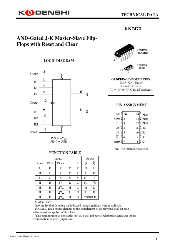
LOGIC DIAGRAM
ORDERING INFORMATION KK7472N Plastic KK7472D SOIC TA = -10° to 70° C for all packages
PIN ASSIGNMENT
PIN 14 =VCC PIN 7 = GND NC
- No internal connection
FUNCTION TABLE
Inputs Reset L H L H H H H Clear H L L H H H H Clock X X X J X X X L H L H K X X X L L H H Output Q H L H
- Q L H H- Q0 L H
Q0 H L
TOGGLE
X =don’t care Q0 = the level of Q before the indicated input conditions were established. TOGGLE: Each output changes to the plement of its previous level on each active transition (pulse) of the clock.
- This configuration is nonstable; that is, it will not persist whenpreset and clear inputs return to their inactive (high) level.
..
MAXIMUM RATINGS-
Symbol VCC VIN IOL Tstg
- Parameter Supply Voltage Input Voltage Low Level Output Current Storage Temperature Range
Value 7.0 5.5 16 -65 to +150
Unit V V m A °C
Maximum Ratings are those values beyond which damage to the device may occur. Functional operation should be restricted to the Remended Operating Conditions.
REMENDED OPERATING CONDITIONS
Symbol VCC VIH VIL IOH IOL tw tsu th fmax TA Supply Voltage High Level Input Voltage Low Level Input Voltage High Level Output Current Low Level Output Current Clock high Pulse Width Input Setup Time Input Hold Time Maximum Clock Frequency Ambient Temperature Range -10 Clock low Reset or Clear low 20 47 25 0↑ 0↓ 15 +70 ns ns MHz °C ns Parameter Min 4.75 2.0 0.8 -400 16 Max 5.25 Unit V V V µA m A
↑↓ The arrow indicates the edge of the clock pulse used for reference: ↑ for the rising edge, ↓ for the falling edge.
..
DC ELECTRICAL CHARACTERISTICS over full operating conditions
Symbol VIK VOH VOL II Parameter Input Clamp Voltage High Level Output Voltage Low Level Output Voltage Input Current at Maximum Input Voltage D, J, K IIH High Level Input Current Clear Reset Clock D, J, K IIL Low Level Input Current IOS- ICC Clear Reset Clock...