KK74ACT273
KK74ACT273 is Common Clock and Reset High-Speed Silicon-Gate CMOS manufactured by Kodenshi AUK Group.
TECHNICAL DATA
..
Octal D Flip-Flop with mon Clock and Reset
High-Speed Silicon-Gate CMOS
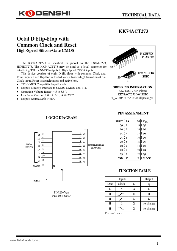
The KK74ACT273 is identical in pinout to the LS/ALS273, HC/HCT273. The KK74ACT273 may be used as a level converter for interfacing TTL or NMOS outputs to High Speed CMOS inputs. This device consists of eight D flip-flops with mon Clock and Reset inputs. Each flip-flop is loaded with a low-to-high transition of the Clock input. Reset is asynchronous and active low.
- TTL/NMOS patible Input Levels
- Outputs Directly Interface to CMOS, NMOS, and TTL
- Operating Voltage Range: 4.5 to 5.5 V
- Low Input Current: 1.0 µA; 0.1 µA @ 25°C
- Outputs Source/Sink 24 m A
ORDERING INFORMATION KK74ACT273N Plastic KK74ACT273DW SOIC TA = -40° to 85° C for all packages
PIN ASSIGNMENT LOGIC DIAGRAM
FUNCTION TABLE
Inputs Reset L PIN 20=VCC PIN 10 = GND H H H H X = don’t care L Clock X D X H L X X Output Q L H L no change no change
..
MAXIMUM RATINGS-
Symbol VCC VIN VOUT IIN IOUT ICC PD Tstg TL
- Parameter DC Supply Voltage (Referenced to GND) DC Input Voltage (Referenced to GND) DC Output Voltage (Referenced to GND) DC Input Current, per Pin DC Output Sink/Source Current, per Pin DC Supply Current, VCC and GND Pins Power Dissipation in Still Air, Plastic DIP+ SOIC Package+ Storage Temperature Lead Temperature, 1 mm from Case for 10 Seconds (Plastic DIP or SOIC Package)
Value -0.5 to +7.0 -0.5 to VCC +0.5 -0.5 to VCC +0.5 ±20 ±50 ±50 750 500 -65 to +150 260
Unit V V V m A m A m A m W °C °C
Maximum Ratings are those values beyond which damage to the device may occur. Functional operation should be restricted to the Remended Operating Conditions. +Derating
- Plastic DIP:
- 10 m W/°C from 65° to 125°C SOIC Package: :
- 7 m W/°C from 65° to 125°C
REMENDED OPERATING CONDITIONS
Symbol VCC VIN, VOUT TJ TA IOH IOL tr, tf
- Parameter DC Supply Voltage (Referenced to GND) DC Input Voltage, Output Voltage (Referenced to GND) Junction Temperature (PDIP) Operating Temperature,...