Kexin Electronics 2KK5081DFN
N-Channel MOSFET
| Part No. | 2KK5081DFN |
|---|---|
| Datasheet | 2KK5081DFN Download |
| Manufacturer | Kexin Electronics |
| Description | N-Channel MOSFET |
| Buy | Stock & Price |
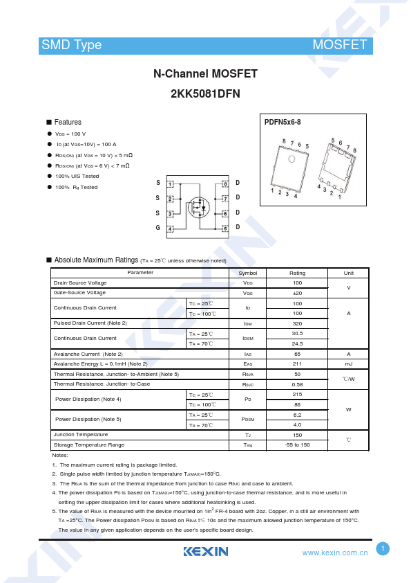
FEATURES
● VDS = 100 V● ID (at VGS=10V) = 100 A
● RDS(ON) (at VGS = 10 V) < 5 mΩ
● RDS(ON) (at VGS = 6 V) < 7 mΩ
● 100% UIS Tested S
● 100% Rg Tested S S G PDFN5x6-8 D D D D
●
ABSOLUTE MAXIMUM RATINGS
(TA = 25℃ unless otherwise noted) Parameter Symbol Rating Unit Drain-Source Voltage Gate-Source Voltage VDS 100 V VGS ±20 Continuous Drain Current TC = 25℃ 100 ID TC = 100℃ 100 A Pulsed Drain Current (Note 2) IDM 320 Continuous Drain Current TA = 25℃ TA = 70℃ IDSM 30.5 24.5 Avalanche Current (Note 2) IAS 65 A Avalanche Energy L = 0.1mH (Note 2) EAS 211 mJ Thermal Resistance, Junction- to-Ambient (Note 5) Thermal Resistance, Junction- to-Case RθJA RθJC 50 0.58 ℃/W Power Dissipation (Note 4) Power Dissipation (Note 5) TC = 25℃ 215 PD TC = 100℃ 86 W TA = 25℃ 6.2 PDSM TA = 70℃ 4.0 Junction Temperature Storage Temperature Range TJ 150 ℃ Tstg -55 to 150 Notes: 1. The maximum current rating is package limited. 2. Single pulse width limited by junction temperature TJ(MAX)=150°C. 3. The RθJA is the sum of the thermal impedance from junction to case RθJC and case to ambient.