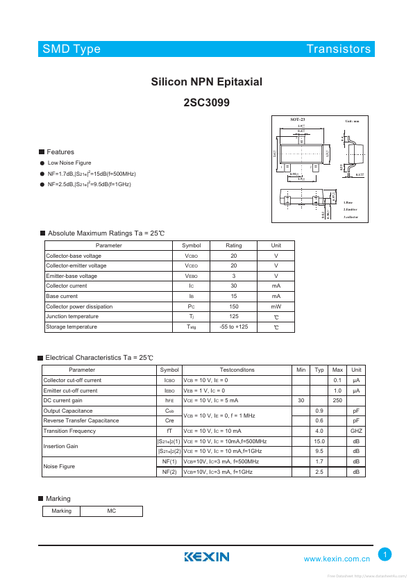
FEATURES
0.4 3 +0.05 0.1-0.01 +0.1 0.97-0.1 1.Base 2.Emitter 3.collector ABSOLUTE MAXIMUM RATINGS
Ta = 25 Parameter Collector-base voltage Collector-emitter voltage Emitter-base voltage Collector current Base current Collector power dissipation Junction temperature Storage temperature Symbol VCBO VCEO VEBO IC IB PC Tj Tstg Rating 20 20 3 30 15 150 125 -55 to +125 Unit V V V mA mA mW ELECTRICAL CHARACTERISTICS
Ta = 25 Parameter Collector cut-off current Emitter cut-off current DC current gain Output Capacitance Reverse Transfer Capacitance Transition Frequency Insertion Gain Symbol ICBO IEBO hFE Cob Cre fT VCE = 10 V, IC = 10 mA Testconditons VCB = 10 V, IE = 0 VEB = 1 V, IC = 0 VCE = 10 V, IC = 5 mA VCB = 10 V, IE = 0, f = 1 MHz 30 0.9 0.6 4.0 15.0 9.5 1.7 2.5 Min Typ Max 0.1 1.0 250 pF pF GHZ dB dB dB dB Unit ìA ìA |S21e|2(1) VCE = 10 V, IC = 10mA,f=500MHz |S21e|2(2) VCE = 10 V, IC = 10 mA,f=1GHz Noise Figure NF(1) NF(2) VCB=10V, IC=3 mA, f=500MHz VCB=10V, IC=3 mA, f=1GHz Marking Mark...