Kexin Electronics 75N08
N-Channel Power MOSFET
| Part No. | 75N08 |
|---|---|
| Datasheet | 75N08 Download |
| Manufacturer | Kexin Electronics |
| Description | N-Channel Power MOSFET |
| Buy | Stock & Price |
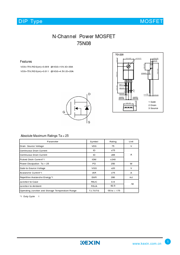
FEATURES
V DS= 75 V,RD S(on)= 0.00 9Ω@ VGS =1 0V ,ID=30A V DS= 75 V,RD S(on)= 0.01 1Ω@ VGS =4 .5V ,ID=20A TO-220 10.16 ±0.20 ø3.18 ±0.10 2.54 ±0.20 (0.70) 3.30 ±0.10 (1.00x45°) 6.68 ±0.20 15.87 ±0.20 15.80 ±0.20 9.75 ±0.30 MAX1.47 0.80 ±0.10 1 23 #1 0.35 ±0.10 2.54TYP [2.54 ±0.20] (30°) 2.54TYP [2.54 ±0.20] 9.40 ±0.20 4.70 ±0.20 0.50 +0.10 –0.05 2.76 ±0.20 1 Gate 2 Drain 3 SourceABSOLUTE MAXIMUM RATINGS
Ta = 25 P aram eter Drain- Source Voltage Continuous Drain Current Continuous Drain Current Pulsed Drain Current*1 Power Dissipation Ta = 25 Gate-to-Source Voltage Avalanche Current*1 Repetitive Avalanche Energy*1 Ju nctio n-to-Cas e Ju nctio n-to-Am bi ent Operating Junction and Storage Temperature Range *1 Duty Cycle 1 S y mbo l VDS ID ID IDM PD VGS IAR EAR RθJC R θJA TJ,TSTG Rating 75 ±75 ±66 ± 240 250 ±20 ±75 280 0. 6 62.5 -55 to + 175 U nit V A W V A mJ /W 1 DSMIPDTTyyppee MOSFICET 75N08ELECTRICAL CHARACTERISTICS
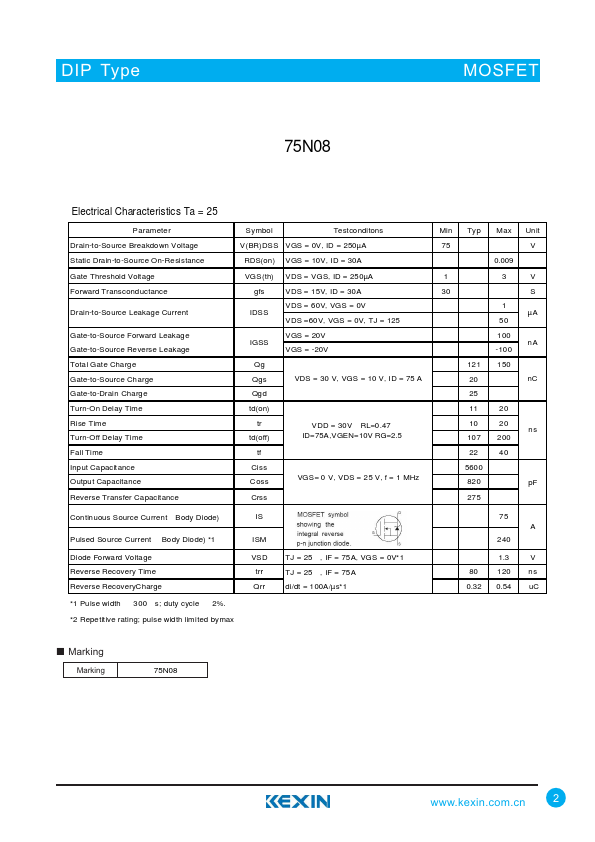
Ta = 25 P aram ete r Drain-to-Source Breakdown Voltage Static Drain...