Datasheet4U.com
🌙
FDN327N Datasheet | Kexin Semiconductor
Part:
FDN327N
Description:
N-Channel MOSFET
Category:
MOSFET
Manufacturer:
Kexin Semiconductor
Size:
1.10 MB
FDN327N Datasheet (PDF) Download
Kexin Semiconductor
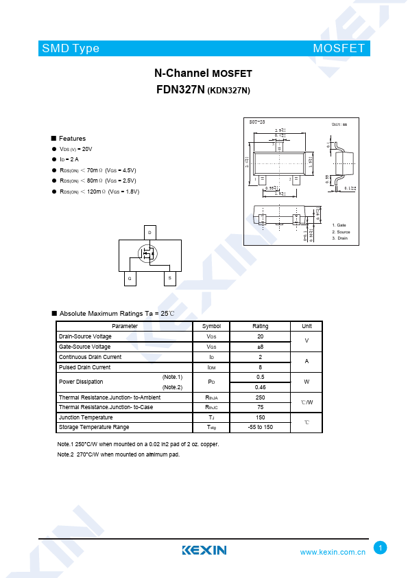
FDN327N
Key Features
VDS (V) = 20V
RDS(ON) < 70mΩ (VGS = 4.5V)
RDS(ON) < 80mΩ (VGS = 2.5V)
0.01 +0.1 0.97 -0.1
Drain 0-0.1 +0.1 0.38
×
Close