Kexin Electronics IRLML5203
P-Channel MOSFET
| Part No. | IRLML5203 |
|---|---|
| Datasheet | IRLML5203 Download |
| Manufacturer | Kexin Electronics |
| Description | P-Channel MOSFET |
| Buy | Stock & Price |
FEATURES
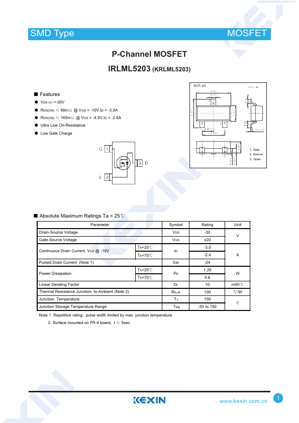
ƽ VDS (V) =-30V ƽ RDS(ON) İ 98mಳ @ VGS = -10V,ID = -3.0A ƽ RDS(ON) İ 165mಳ @ VGS = -4.5V,ID = -2.6A ƽ Ultra Low On-Resistance ƽ Low Gate Charge +0.1 2.4 -0.1 SOT-23 2.9 +0.1 -0.1 0.4 +0.1 -0.1 3 1 2 0.95 +0.1 -0.1 1.9 +0.1 -0.1 +0.1 1.3 -0.1 0.55 0.4 Unit: mm 0.1 +0.05 -0.01 +0.1 0.97 -0.1 1. Gate 2. Source 3. Drain 0-0.1 +0.1 0.38 -0.1 ƵABSOLUTE MAXIMUM RATINGS
Ta = 25ć Drain-Source Voltage Gate-Source Voltage Parameter Continuous Drain Current, VGS @ -10V Pulsed Drain Current (Note 1) Power Dissipation Linear Derating Factor Thermal Resistance.Junction- to-Ambient (Note 2) Junction Temperature Junction Storage Temperature Range TA=25ć TA=70ć TA=25ć TA=70ć Symbol VDS VGS ID IDM PD DL RthJA TJ Tstg Note 1. Repetitive rating; pulse width limited by max. junction temperature. 2. Surface mounted on FR-4 board, t İ 5sec. Rating -30 ±20 -3.0 -2.4 -24 1.25 0.8 10 100 150 -55 to 150 Unit V A W mW/ć ć/W ć 1 SMD Type TraMnOsiSstFoErsT P-Channel MOSFET IRLML5203 (KRLML5203) ƵELECTRICAL CHARACTERISTICS
@ TJ = 25ć(unless otherwise specified) Parameter Drain-Source Breakdown Voltage Breakdown Voltage Temp.