Datasheet4U Logo Datasheet4U.com

KDB2532 - N-Channel MOSFET

Key Features

  • rDS(ON) = 14m (Typ. ), VGS = 10V, ID = 33A Qg(tot) = 82nC (Typ. ), VGS = 10V Low Miller Charge Low QRR Body Diode UIS Capability (Single Pulse and Repetitive Pulse) +0.25.28 -0.2 +0.28.7 -0.2 TO-263 +0.2 4.57+0.1 -0.2 1.27-0.1 Unit: mm +0.11.27 -0.1 +0.22.54 -0.2 15.25-+00..22 5.60 1.27+0.1 -0.1 0.1max 2.54+0.2 -0.2 5.08+0.1 -0.1 0.81+0.1 -0.1 2.54 0.4+0.2 -0.2 1 Gate 2 Drain 3 Source Absolute Maximum Ratings Ta = 25 Parameter Drain to source voltage Gate to source voltage Drain curr.

📥 Download Datasheet

Full PDF Text Transcription for KDB2532 (Reference)

Note: Below is a high-fidelity text extraction (approx. 800 characters) for KDB2532. For precise diagrams, and layout, please refer to the original PDF.

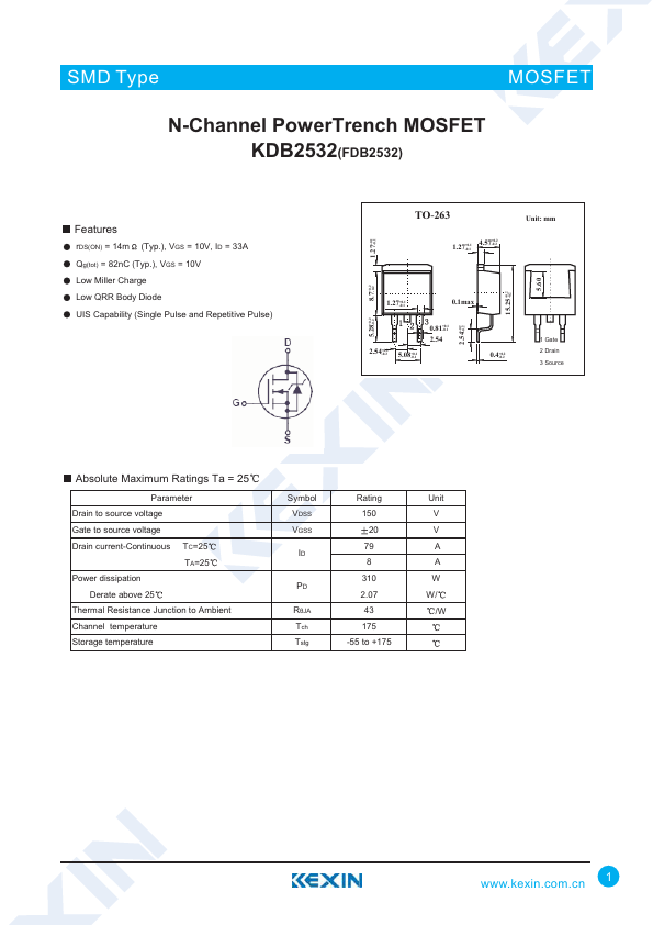
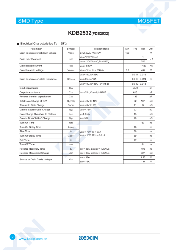
SMD Type MOSFET N-Channel PowerTrench MOSFET KDB2532(FDB2532) Features rDS(ON) = 14m (Typ.), VGS = 10V, ID = 33A Qg(tot) = 82nC (Typ.), VGS = 10V Low Miller Charge Low QR...

View more extracted text
0V, ID = 33A Qg(tot) = 82nC (Typ.), VGS = 10V Low Miller Charge Low QRR Body Diode UIS Capability (Single Pulse and Repetitive Pulse) +0.25.28 -0.2 +0.28.7 -0.2 TO-263 +0.2 4.57+0.1 -0.2 1.27-0.1 Unit: mm +0.11.27 -0.1 +0.22.54 -0.2 15.25-+00..22 5.60 1.27+0.1 -0.1 0.1max 2.54+0.2 -0.2 5.08+0.1 -0.1 0.81+0.1 -0.1 2.54 0.4+0.2 -0.2 1 Gate 2 Drain 3 Source Absolute Maximum Ratings Ta = 25 Parameter Drain to source voltage Gate to source voltage Drain current-Continuous TC=25 TA=25 Power dissipation Derate above 25 Thermal Resistance Junction to Ambient Channel temperature Storage temperature Symbol VDSS VGSS ID PD RèJA Tch T