KDB4020P
Features
-16 A, -20 V. RDS(on) = 0.08 Ù @ VGS = -4.5 V RDS(on) = 0.11 Ù @ VGS = -2.5 V.
Critical DC electrical parameters specified at elevated temperature. High density cell design for extremely low RDS(on).
+0.25.28 -0.2
+0.28.7 -0.2
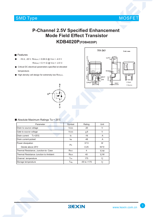
TO-263
+0.2
4.57+0.1 -0.2 1.27-0.1
Unit: mm
+0.11.27 -0.1
+0.22.54 -0.2 15.25-+00..22 5.60
1.27+0.1 -0.1
0.1max
2.54+0.2 -0.2
5.08+0.1 -0.1
0.81+0.1 -0.1
0.4+0.2 -0.2
1 Gate 2 Drain 3 Source
Absolute Maximum Ratings Ta = 25
Parameter Drain to source voltage Gate to source voltage Drain current TC=25 Drain current-pulsed Power dissipation
Derate above 25 Thermal Resistance, Junction-to- Case Thermal Resistance Junction to Ambient Channel temperature Storage temperature
Symbol VDSS VGSS ID Idp
RèJC RèJA Tch Tstg
Rating -20 8 -16 -48 37.5 0.25 4 40 175
-55 to +175
Unit V V A A W
W/ /W /W
.kexin..cn 1
SMD Type
KDB4020P(FDB4020P)
Electrical Characteristics Ta = 25
Parameter Drain to source breakdown voltage Drain cut-off current...