Datasheet4U.com
🌙
KI2301DS-HF Datasheet | Kexin Semiconductor
Part:
KI2301DS-HF
Description:
P-Channel MOSFET
Category:
MOSFET
Manufacturer:
Kexin Semiconductor
Size:
1.46 MB
KI2301DS-HF Datasheet (PDF) Download
Related KI2301DS-HF Datasheets
KI2301DS P-Channel MOSFET
KI2301T P-Channel MOSFET
KI2301 P-Channel MOSFET
KI2302DS N-Channel MOSFET
KI2307DS P-Channel MOSFET
Kexin Semiconductor
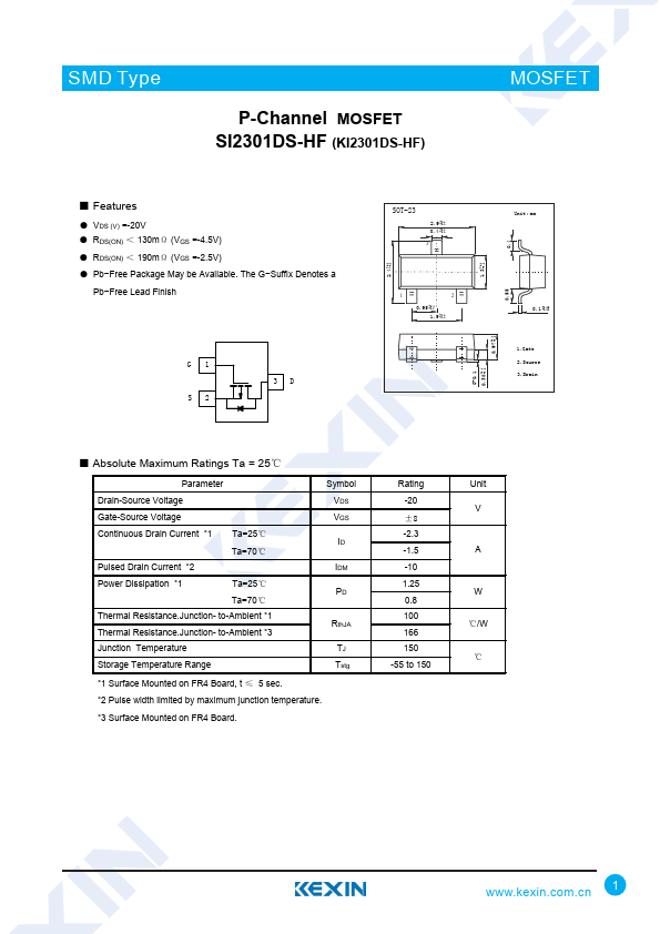
KI2301DS-HF
Key Features
VDS (V) =-20V
RDS(ON) < 130mΩ (VGS =-4.5V)
RDS(ON) < 190mΩ (VGS =-2.5V)
Pb−Free Package May be Available. The G−Suffix Denotes a
×
Close