KI30P03DFN
Features
- VDS (V) =-30V
- ID =-30 A (VGS =±20V)
- RDS(ON) <15mΩ (VGS =-10V)
- RDS(ON) <25mΩ (VGS =-4.5V)
MOSFET xxxxxxxxxxx
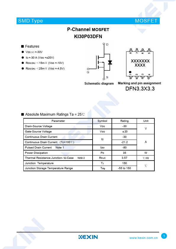
Schematic diagram Marking and pin assignment
DFN3.3X3.3
- Absolute Maximum Ratings Ta = 25℃
Parameter Drain-Source Voltage Gate-Source Voltage Continuous Drain Current Continuous Drain Current (TC=100℃) Pulsed Drain Current Note 1 Power Dissipation Thermal Resistance.Junction- to-Case Junction Temperature Junction Storage Temperature Range
Note 2
Symbol VDS VGS
IDM PD Rth JC TJ Tstg
Rating -30 ± 20 -30 -21.2 -80 35 3.57 150
-55 to 150
Unit V
W ℃/W
℃
.kexin..cn 1
SMD Type
MOSFET
P-Channel MOSFET
- Electrical Characteristics Ta = 25℃
Parameter Drain-Source Breakdown Voltage Zero Gate Voltage Drain Current Gate-Body Leakage Current Gate Threshold Voltage
Static Drain-Source On-Resistance
Forward Transconductance Input Capacitance Output Capacitance Reverse Transfer Capacitance Total Gate Charge Gate Source Charge Gate Drain Charge Turn-On Delay Time...