KI9926A
KI9926A is Dual N-Channel MOSFET manufactured by Kexin Semiconductor.
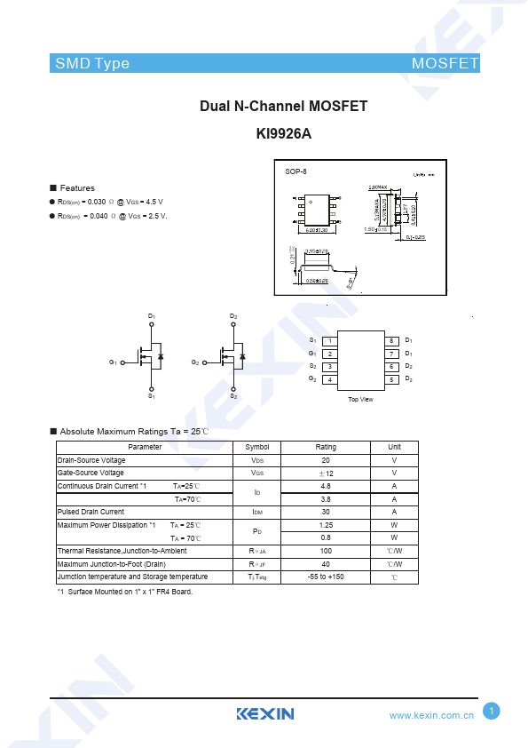
SMD Type
MOSFET
- Features
- RDS(on) = 0.030 Ω @ VGS = 4.5 V
- RDS(on) = 0.040 Ω @ VGS = 2.5 V.
Dual N-Channel MOSFET KI9926A
SOP-8
1.50 0.15
+0.040.21 -0.02
D1 D2
G1 G2
S1 S2
-...