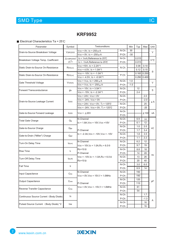
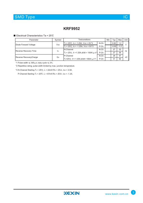
Kexin Electronics KRF9952
HEXFET Power MOSFET
| Part No. | KRF9952 |
|---|---|
| Datasheet | KRF9952 Download |
| Manufacturer | Kexin Electronics |
| Description | HEXFET Power MOSFET |
| Buy | Stock & Price |

FEATURES
Generation V Technology Ultra Low On-Resistance Dual N and P Channel MOSFET Surface Mount Very Low Gate Charge and Switching Losses Fully Avalanche Rated 1 : Source1 2 : Gate1 3 : Source2 4 : Gate2 5 : Drain2 6 : Drain2 7 : Drain1 8 : Drain1ABSOLUTE MAXIMUM RATINGS
Ta = 25 Parameter Drain-Source Voltage Gate-to-Source Voltage Continuous Drain Current, VGS @ 10V @ Ta = 25 Continuous Drain Current, VGS @ 10V @ Ta = 70 Pulsed Drain Current *1 Continuous Source Current (Diode Conduction) Power Dissipation Power Dissipation @Ta= 25 @Ta= 70 EAS IAR EAR dv/dt TJ, TSTG R JA Symbol VDS VGS ID ID IDM IS PD N-Channel 30 20 3.5 2.8 16 1.7 2 1.3 44 2.0 0.25 5.0 P-Channel Unit V V -2.3 -1.8 -10 -1.3 A W 57 -1.3 mJ A mJ -5 -55 to + 150 62.5 /W V/ns A Single Pulse Avalanche Energy Avalanche Current Repetitive Avalanche Energy Peak Diode Recovery dv/dt *2 Junction and Storage Temperature Range Maximum Junction-to-Ambient *3 *1 Repetitive rating; pulse width limited by max. junction temperature. *2 N-Channel ISD P-Channel ISD 2.0A, di/dt -1.3A, di/dt 100A/ 84A/ s, VDD s, VDD 10sec.