Kexin Electronics OB2263
The PWM duty cycle is determined by voltage level into this pin and SENSE pin input.| Part No. | OB2263 |
|---|---|
| Datasheet | OB2263 Download |
| Manufacturer | Kexin Electronics |
| Description | Current Mode PWM Controller |
| Buy | Stock & Price |
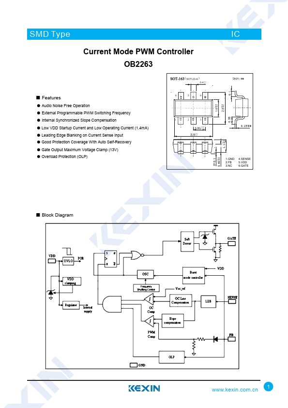
FEATURES
● Audio Noise Free Operation● External Programmable PWM Switching Frequency
● Internal Synchronized Slope Compensation
● Low VDD Startup Current and Low Operating Current (1.4mA)
● Leading Edge Blanking on Current Sense Input
● Good Protection Coverage With Auto Self-Recovery
● Gate Output Maximum Voltage Clamp (13V)
● Overload Protection (OLP) 6 54 1 23 +0.01 -0.01 +0.2 -0.1 0-0.1 +0.10.68 -0.1 +0.21.6 -0.1 +0.22.8 -0.1 +0.11.1 -0.1 IC Unit: mm 0.4 0.55 0.15 +0.02 -0.02 1.GND 2.FB 3.NC 4.SENSE 5.VDD 6.GATE
● Block Diagram 1 SMD Type Current Mode PWM Controller OB2263
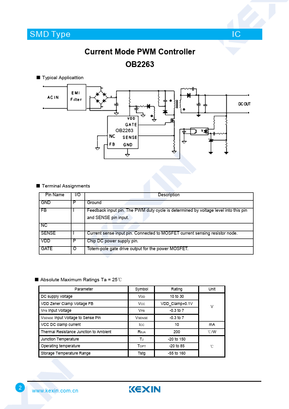
● Typical Applicattion IC OB2263
● Terminal Assignments Pin Name GND FB NC SENSE VDD GATE I/O
DESCRIPTION
P Ground I Feedback input pin. I Current sense input pin. Connected to MOSFET current sensing resistor node. P Chip DC power supply pin. O Totem-pole gate drive output for the power MOSFET.●
ABSOLUTE MAXIMUM RATINGS
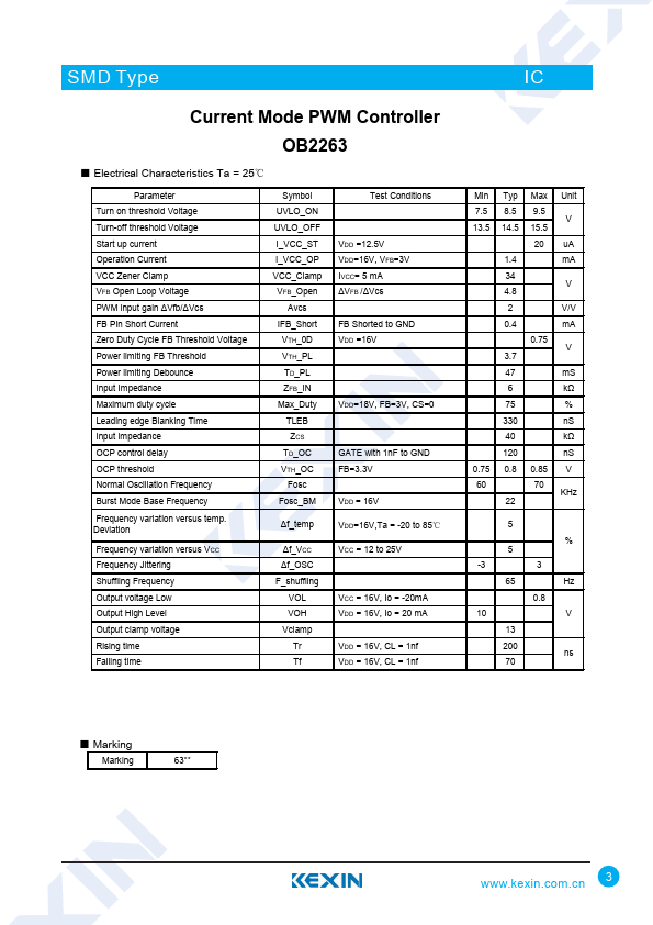
Ta = 25℃ Parameter DC supply voltage VDD Zener Clamp Voltage FB VFB Input Voltage VSENSE Inp...