SI2337DS
SI2337DS is P-Channel Enhancement MOSFET manufactured by Kexin Semiconductor.
Features
- VDS (V) =-80V
- ID =-2.2A (VGS =-10V)
- RDS(ON) < 270mΩ (VGS =-10V) S
- RDS(ON) < 303mΩ (VGS =-6V)
G1 S2
G 3D
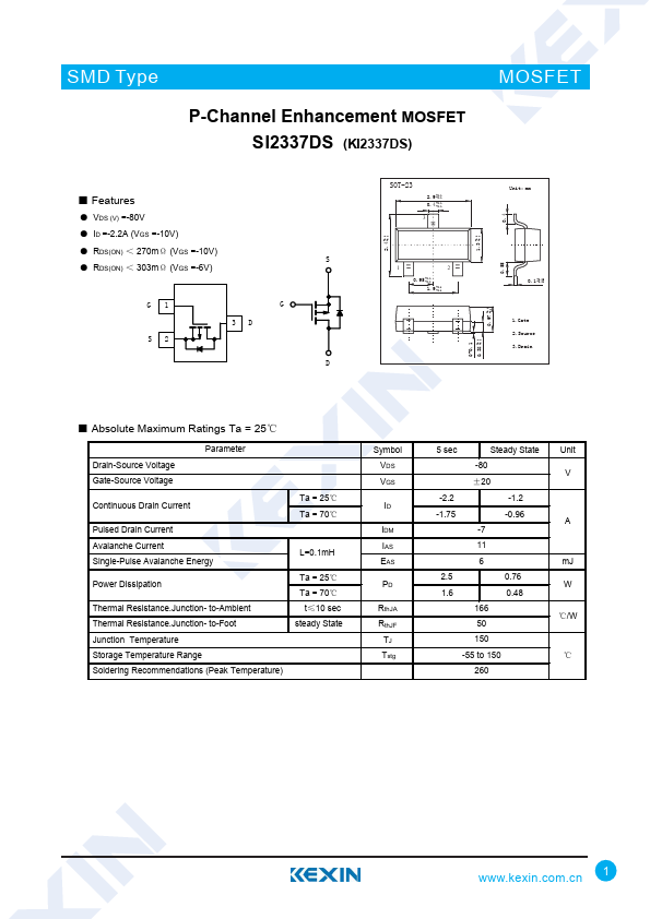
+0.1 2.4 -0.1
SOT-23
2.9 +0.1 -0.1
0.4 +0.1 -0.1
0.95 +0.1 -0.1 1.9 +0.1 -0.1
0-0.1 +0.1 0.38
-0.1
+0.1 1.3 -0.1
+0.1 0.97 -0.1
Unit: mm
0.1 +0.05 -0.01
1.Gate 2.Source 3.Drain
- Absolute Maximum Ratings Ta = 25℃
Drain-Source Voltage Gate-Source Voltage
Parameter
Continuous Drain Current
Pulsed Drain Current Avalanche Current Single-Pulse Avalanche Energy
Power Dissipation
Thermal Resistance.Junction- to-Ambient Thermal Resistance.Junction- to-Foot Junction Temperature Storage Temperature Range Soldering Remendations (Peak Temperature)
Ta = 25℃ Ta = 70℃
L=0.1m H
Ta = 25℃ Ta = 70℃ t≤10 sec steady State
Symbol VDS VGS
IDM IAS EAS
Rth JA Rth...