KHX1333C9D3B1-4G
Description
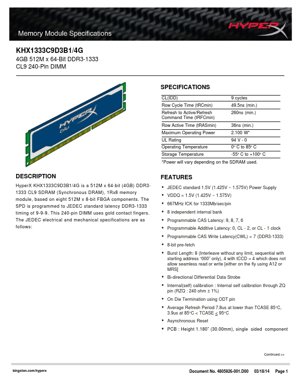
HyperX KHX1333C9D3B1/4G is a 512M x 64-bit (4GB) DDR31333 CL9 SDRAM (Synchronous DRAM), 1Rx8 memory module, based on eight 512M x 8-bit FBGA ponents.
Key Features
- Continued >>
HyperX KHX1333C9D3B1/4G is a 512M x 64-bit (4GB) DDR31333 CL9 SDRAM (Synchronous DRAM), 1Rx8 memory module, based on eight 512M x 8-bit FBGA ponents.