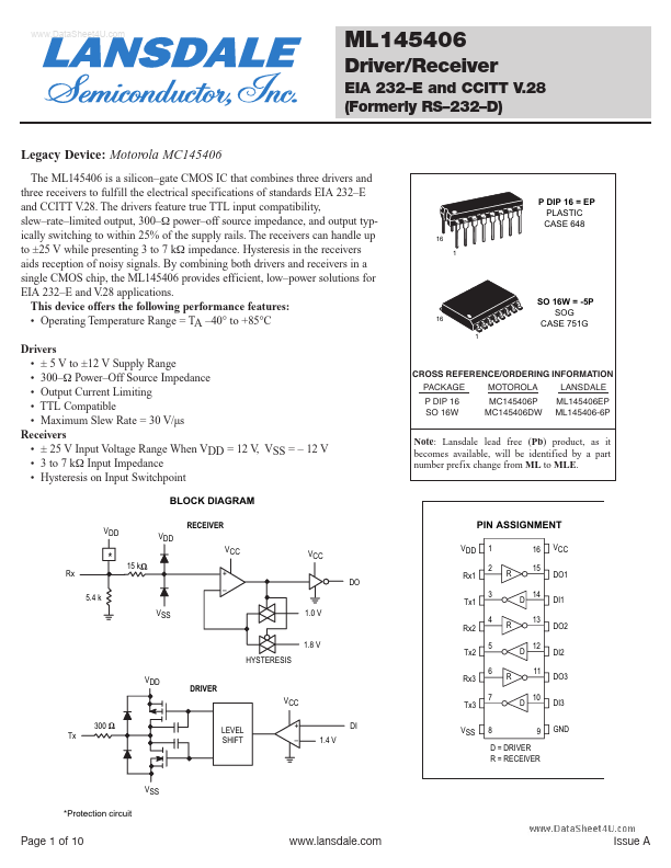
Datasheet4U Logo Datasheet4U.com

ML145406 - Driver/Receiver

Description

VDD Positive Power Supply (Pin 1) The most positive power supply pin, which is typically + 5 to +12V.

5 to

12 V.

Features

  • Operating Temperature Range = TA.
  • 40° to +85°C Drivers.
  • ± 5 V to ±12 V Supply Range.
  • 300.
  • Ω Power.
  • Off Source Impedance.
  • Output Current Limiting.
  • TTL Compatible.
  • Maximum Slew Rate = 30 V/µs Receivers.
  • ± 25 V Input Voltage Range When VDD = 12 V , VSS =.
  • 12 V.
  • 3 to 7 kΩ Input Impedance.
  • Hysteresis on Input Switchpoint BLOCK.

📥 Download Datasheet

Datasheet preview – ML145406

Datasheet Details

Part number ML145406
Manufacturer LANSDALE Semiconductor
File Size 512.63 KB
Description Driver/Receiver
Datasheet download datasheet ML145406 Datasheet
Additional preview pages of the ML145406 datasheet.
Other Datasheets by LANSDALE Semiconductor

Full PDF Text Transcription

Click to expand full text
www.DataSheet4U.com ML145406 Driver/Receiver EIA 232–E and CCITT V.28 (Formerly RS–232–D) Legacy Device: Motorola MC145406 The ML145406 is a silicon–gate CMOS IC that combines three drivers and three receivers to fulfill the electrical specifications of standards EIA 232–E and CCITT V .28. The drivers feature true TTL input compatibility, slew–rate–limited output, 300–Ω power–off source impedance, and output typically switching to within 25% of the supply rails. The receivers can handle up to ±25 V while presenting 3 to 7 kΩ impedance. Hysteresis in the receivers aids reception of noisy signals. By combining both drivers and receivers in a single CMOS chip, the ML145406 provides efficient, low–power solutions for EIA 232–E and V .28 applications.
Published: |