CESD3V3D7
CESD3V3D7 is ESD Protection Diodes manufactured by LGE.
DESCRIPTION
The CESD3V3D7 is designed to protect voltage sensitive ponents from ESD. Excellent clamping capability, low leakage, and fast response time provide best in class protection on designs that are exposed to ESD. Because of its small size, it is suited for use in cellular phones, MP3 players, digital cameras and many other portable applications where board space is at a premium.
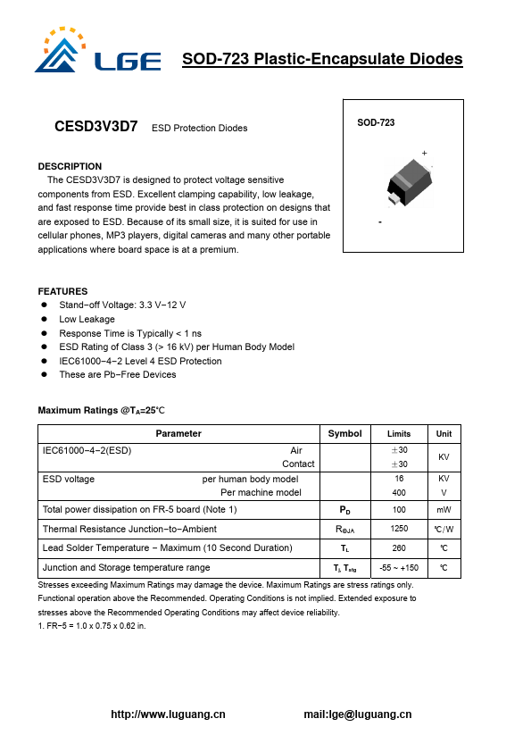
SOD-723
- +
FEATURES z Stand- off Voltage: 3.3 V- 12 V z Low Leakage z Response Time is Typically < 1 ns z ESD Rating of Class 3 (> 16 k V) per Human Body Model z IEC61000- 4- 2 Level 4 ESD Protection z These are Pb- Free Devices
Maximum Ratings @TA=25℃
IEC61000- 4- 2(ESD) ESD voltage
Parameter
Air Contact per human body model Per machine model
Symbol
Limits
±30 ±30 16 400
Total power dissipation on FR-5 board (Note 1)
PD 100
Thermal Resistance Junction- to- Ambient
RΘJA
Lead Solder Temperature
- Maximum (10 Second Duration)
TL 260
Junction and Storage temperature range
Tj, Tstg
-55 ~ +150
Stresses exceeding Maximum Ratings may damage the device. Maximum Ratings are stress ratings only. Functional operation above the Remended. Operating Conditions is not implied. Extended exposure to stresses above the Remended Operating Conditions may affect device reliability. 1. FR- 5 = 1.0 x 0.75 x 0.62 in.
Unit
KV V m W ℃/W ℃ ℃ http://.luguang.cn mail:lge@luguang.cn
ELECTRICAL CHARACTERISTICS (TA = 25°C unless otherwise noted)
Symbol
IPP VC VRWM IR VBR IT IF VF Ppk C
Parameter
Maximum Reverse Peak Pulse Current Clamping Voltage @ IPP Working Peak Reverse Voltage Maximum Reverse Leakage Current @ VRWM Breakdown Voltage @ IT Test Current Forward Current Forward Voltage @ IF Peak Power Dissipation Max. Capacitance @VR=0 and f =1MHz
ELECTRICAL CHARACTERISTICS (TA = 25°C unless otherwise noted, VF = 0.9 V Max. @ IF = 10m A for all types)
Device-
Device Marking
VRWM (V) Max
IR (μA) @ VRWM Max
VBR (V) @ IT(Note 2) Min Max
IT m A
IPP(A) +...