Datasheet4U Logo Datasheet4U.com

LSK389B - Ultra Low Noise Monolithic Dual N-Channel JFET Amplifier

Download the LSK389B datasheet PDF. This datasheet also covers the LSK389 variant, as both devices belong to the same ultra low noise monolithic dual n-channel jfet amplifier family and are provided as variant models within a single manufacturer datasheet.

General Description

The LSK389 Series, Monolithic Dual N-Channel JFETs were specifically designed to provide users a better performing, less time consuming and cheaper solution for obtaining tighter IDSS matching, and better thermal tracking, than matching individual JFETs.

Key Features

  • Ultra Low Noise: en = 1.9nV/√Hz (typ), f = 1kHz and NBW = 1Hz.
  • Tight Matching: IVGS1-2I = 20mV max.
  • High Breakdown Voltage: BVGSS = 40V max.
  • High Gain: Gfs = 20mS (typ).
  • Low Capacitance: 25pF typ.
  • Improved Second Source Replacement for 2SK389 Benefits.
  • Unique Monolithic Dual Design Construction of Interleaving Both JFETs on the Same Piece of Silicon.
  • Excellent Matching and Thermal Tracking.
  • Great for Maximizing Battery Operated.

📥 Download Datasheet

Note: The manufacturer provides a single datasheet file (LSK389-LINEARSYSTEMS.pdf) that lists specifications for multiple related part numbers.

Datasheet Details

Part number LSK389B
Manufacturer LINEAR SYSTEMS
File Size 718.52 KB
Description Ultra Low Noise Monolithic Dual N-Channel JFET Amplifier
Datasheet download datasheet LSK389B Datasheet

Full PDF Text Transcription (Reference)

The following content is an automatically extracted verbatim text from the original manufacturer datasheet and is provided for reference purposes only.

View original datasheet text
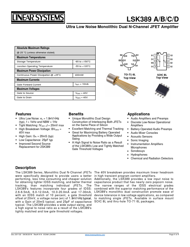
LSK389 A/B/C/D Ultra Low Noise Monolithic Dual N-Channel JFET Amplifier Absolute Maximum Ratings @ 25 °C (unless otherwise stated) Maximum Temperatures Storage Temperature Junction Operating Temperature Maximum Power Dissipation Continuous Power Dissipation @ +25°C Maximum Currents Gate Forward Current Maximum Voltages Gate to Source Gate to Drain -65 to +150°C -55 to +135°C 400mW IG(F) = 10mA VGSS = 40V VGDS = 40V S2 4 D2 5 G2 6 3 G1 2 D1 1 S1 TO-71 6L Top View SOIC 8L Top View Features  Ultra Low Noise: en = 1.