LOGIC DEVICES LF3324
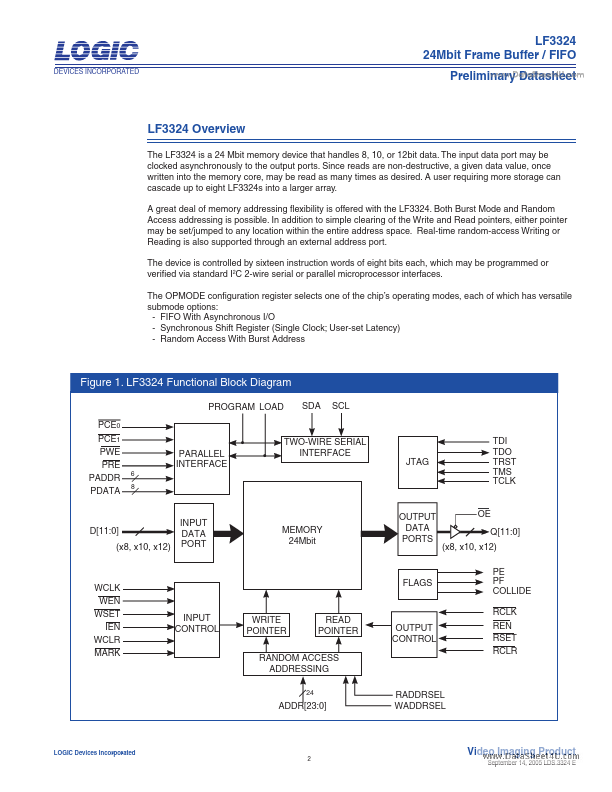
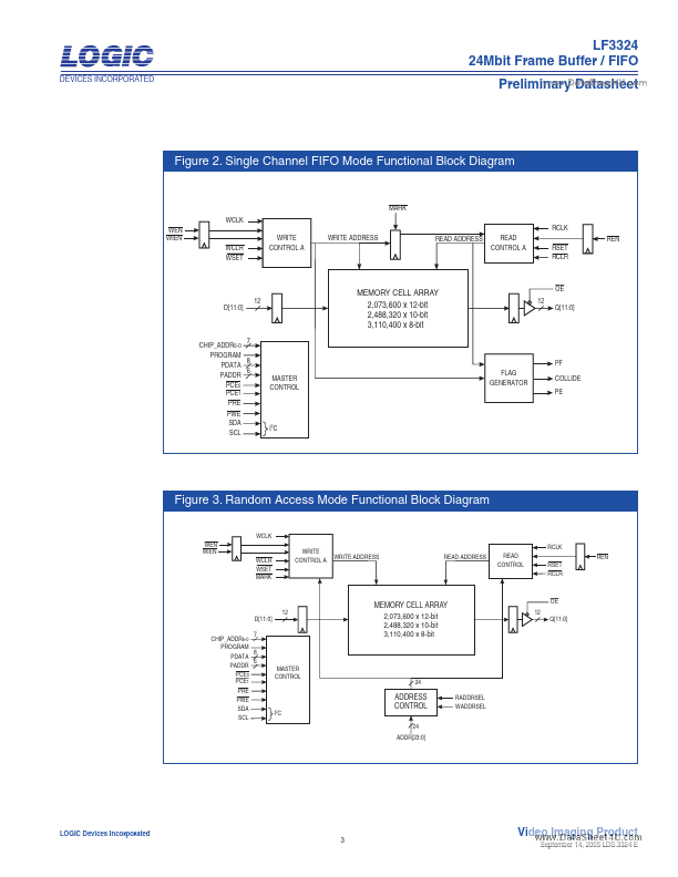
The LF3324 is a 24 Mbit memory device that handles 8, 10, or 12bit data. The input data port may be clocked asynchronously to the output ports. Random Access Mode Functional Block Diagram WCLK WEN WIEN WCLR WSET MARK WRITE CONTROL A RCLK WRITE ADDRESS READ ADDRESS READ CONTROL REN RSET RCLR D[11:0] CHIP_ADDR6-0 PROGRAM PDATA 7 8 12 MEMORY CELL ARRAY 2,073,600 x 12-bit 2,488,320 x 10-bit 3,110,400 x 8-bit OE 12 Q[11:0] PADDR PCE0 PCE1 PRE 6...| Part No. | LF3324 |
|---|---|
| Datasheet | LF3324 Download |
| Manufacturer | LOGIC DEVICES |
| Description | 24Mbit Frame Buffer/FIFO |
| Buy | Stock & Price |
FEATURES
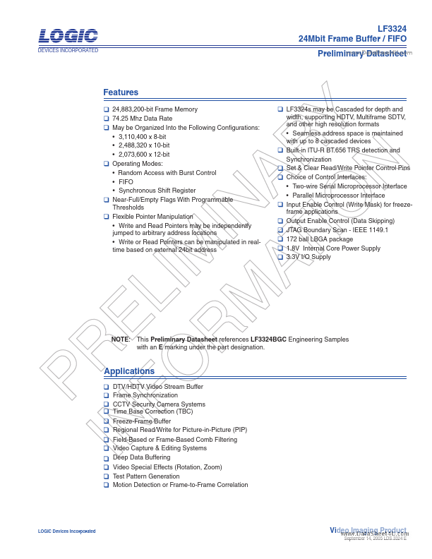
24,883,200-bit Frame Memory 74.25 Mhz Data Rate May be Organized Into the Following Configurations:● 3,110,400 x 8-bit
● 2,488,320 x 10-bit
● 2,073,600 x 12-bit Operating Modes:
● Random Access with Burst Control
● FIFO
● Synchronous Shift Register Near-Full/Empty Flags With Programmable Thresholds Flexible Pointer Manipulation
● Write and Read Pointers may be independently jumped to arbitrary address locations
● Write or Read Pointers can be manipulated in realtime based on external 24bit address LF3324s may be Cascaded for depth and width, supporting HDTV, Multiframe SDTV, and other high resolution formats
● Seamless address space is maintained with up to 8 cascaded devices Built-in ITU-R BT.656 TRS detection and Synchronization Set & Clear Read/Write Pointer Control Pins Choice of Control Interfaces:
● Two-wire Serial Microprocessor Interface
● Parallel Microprocessor Interface Input Enable Control (Write Mask) for freezeframe applications Output Enable Control (Data Skipp...