DESCRIPTION
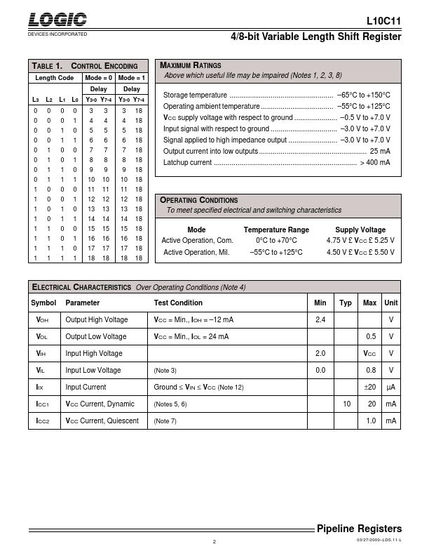
Both shift registers can be programmed together to any length from 3 to 18 stages inclusive, or one register can be fixed at 18 stages of delay while the other is variable. The configuration implemented is determined by the Length Code (L 3-0) and the MODE control line as shown in Table 1. Each input is applied to a chain of registers which are clocked on the rising edge of the common CLK input. These registers are numbered R1 through R17 and R1’ through R17’, corresponding to the D 3-0 and D 7-4 data fields respectively. A multiplexer serves to route the contents of any of registers R2 through R17 to the output register, denoted R18. A similar multiplexer operates on the contents of R2’ through R17’ to load R18’. Note that the minimum-length path from data inputs to outputs is R1 to R2 to R18, consisting of three stages of delay. The MODE input determines whether one or both of the internal shift registers have variable length. When MODE = 0, both D 3-0 and D 7-4 are delayed by an amount which is controlled by L3-0. LOGIC Devices Incorporated