DESCRIPTION
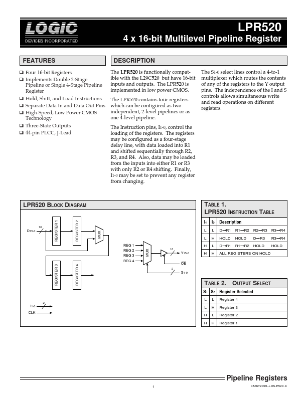
The LPR520 is implemented in low power CMOS. The Instruction pins, I1-0, control the loading of the registers. The registers may be configured as a four-stage delay line, with data loaded into R1 and shifted sequentially through R2, R3, and R4. Also, data may be loaded from the inputs into either R1 or R3 with only R2 or R4 shifting. Finally, I1-0 may be set to prevent any register from changing. The S1-0 select lines control a 4-to-1 multiplexer which routes the contents of any of the registers to the Y output pins. The independence of the I and S controls allows simultaneous write and read operations on different registers. FEATURES
u Four 16-bit Registers u Implements Double 2-Stage Pipeline or Single 4-Stage Pipeline Register u Hold, Shift, and Load Instructions u Separate Data In and Data Out Pins u High-Speed, Low Power CMOS Technology u Three-State Outputs u 44-pin PLCC, J-Lead LPR520 BLOCK DIAGRAM REGISTER 1 REGISTER 2 TABLE 1. LPR520 INSTRUCTION TABLE I1 MUX I0 L H... LOGIC Devices Incorporated