L74VHC1GT03
L74VHC1GT03 is 2-Input NOR Gate with Open Drain Output manufactured by LRC.
LESHAN RADIO PANY, LTD.
2- Input NOR Gate with Open Drain Output with LSTTL- patible Inputs
The L74VHC1GT03 is an advanced high speed CMOS 2- input NOR gate with an open drain output fabricated with silicon gate CMOS technology. It achieves high speed peration similar to equivalent Bipolar Schottky TTL while maintaining CMOS low power dissipation. The internal circuit is posed of three stages, including an open drain output which provides the ability to set output switching level. This allows the L74VHC1GT03 to be used to interface 5 V circuits to circuits of any voltage between V CC and 7 V using an external resistor and power supply. The device input is patible with TTL- type input thresholds and the output has a full 5.0 V CMOS level output swing. The input protection circuitry on this device allows overvoltage tolerance on the input, allowing the device to be used as a logic- level translator from 3.0 V CMOS logic to 5.0 V CMOS Logic or from 1.8 V CMOS logic to 3.0 V CMOS Logic while operating at the high- voltage power supply. The L74VHC1GT03 input structure provides protection when voltages up to 7 V are applied, regardless of the supply voltage. This allows the L74VHC1GT03 to be used to interface 5 V circuits to 3 V circuits. The output structures also provide protection when V CC = 0 V. These input and output structures help prevent device destruction caused by supply voltage
- input/output voltage mismatch, battery backup, hot insertion, etc.
- High Speed: t PD = 3.6 ns (Typ) at V CC = 5 V
- Low Internal Power Dissipation: I CC = 2 m A (Max) at T A = 25°C
- Power Down Protection Provided on Inputs
- Pin and Function patible with Other Standard Logic Families
- Chip plexity: FETs = 62; Equivalent Gates = 16
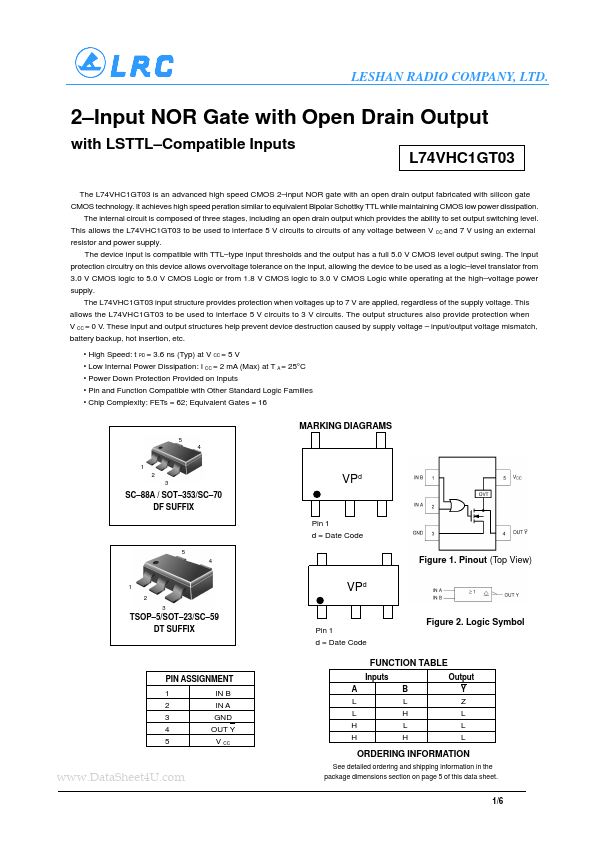
MARKING DIAGRAMS
5 4 1 2 3
VPd
SC- 88A / SOT- 353/SC- 70 DF SUFFIX Pin 1 d = Date Code
5 4
Figure 1. Pinout (Top View)
1 2 3
VPd
Figure 2. Logic Symbol
Pin 1 d = Date Code
TSOP- 5/SOT- 23/SC- 59 DT SUFFIX
FUNCTION TABLE
PIN ASSIGNMENT 1 2 3 4 5...