LS7084
LS7084 is QUADRATURE CLOCK CONVERTER manufactured by LSI Computer Systems.
FEATURES
:
- x1 and x4 mode selection
- Up to 16 MHz output clock frequency
- Programmable output clock pulse width
- On-chip filtering of inputs for optical or magnetic encoder applications.
- TTL and CMOS patible I/Os
- +4.5V to +10.0V operation (VDD-VSS)
- LS7083, LS7084 (DIP) LS7083-S, LS7084-S (SOIC)
- See Figure 1 DESCRIPTION
: The LS7083 and LS7084 are monolithic CMOS silicon gate quadrature clock converters. Quadrature clocks derived from optical or magnetic encoders, when applied to the A and B inputs of the LS7083/LS7084, are converted to strings of Up Clocks and Down Clocks (LS7083) or to a Clock and an Up/Down direction control (LS7084). These outputs can be interfaced directly with standard Up/Down counters for direction and position sensing of the encoder. INPUT/OUTPUT DESCRIPTION
: RBIAS (Pin 1) Input for external ponent connection. A resistor connected between this input and V SS adjusts the output clock pulse width (Tow). For proper operation, the output clock pulse width must be less than or equal to the A,B pulse separation (TOW≤TPS). VDD (Pin 2) Supply Voltage positive terminal. VSS (Pin 3) Supply Voltage negative terminal. A (Pin 4) Quadrature Clock Input A. This input has a filter circuit to validate input logic level and eliminate encoder dither. B (Pin 5) Quadrature Clock Input B. This input has a filter circuit identical to input A. x4/x1 (Pin 6) This input selects between x1 and x4 modes of operation. A high-level selects x4 mode and a low-level selects the x1 mode. In x4 mode, an output pulse is generated for every transition at either A or B input. In x1 mode, an output pulse is generated in one bined A/B input cycle. (See Figure 2.)
7083/84-100600-1
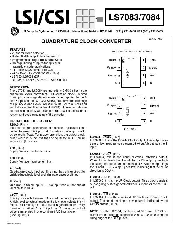
PIN ASSIGNMENT
- TOP VIEW
LSI LS7083 LSI LS7084
FIGURE 1
RBIAS
8 7 6
UPCK
V DD(+V) 2 VSS(-V) 3 A 4
DNCK x4/x1
RBIAS V DD(+V)
1 2
8 7 6
UP/DN x4/x1
VSS(-V) 3 A
LS7083
- DNCK (Pin 7) In LS7083, this is the DOWN Clock Output. This output consists of low-going...