LSI Computer Systems LS7184
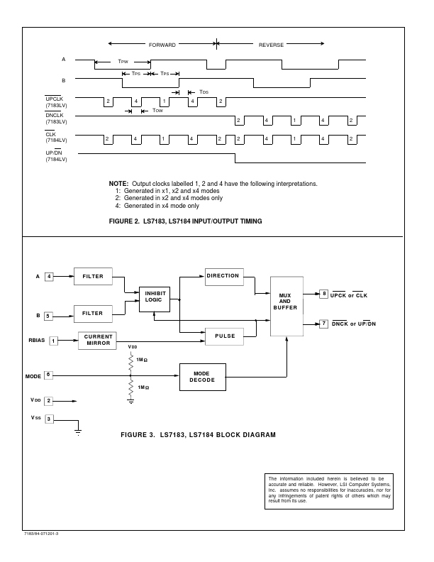
the LS7184, the timing of CLK and UP/DN requires that the counter interfacing with LS7184 counts on the rising edge of the CLK pulses.| Part No. | LS7184 |
|---|---|
| Datasheet | LS7184 Download |
| Manufacturer |  LSI Computer Systems |
| Description | QUADRATURE CLOCK CONVERTER |
| Buy | Stock & Price |
FEATURES
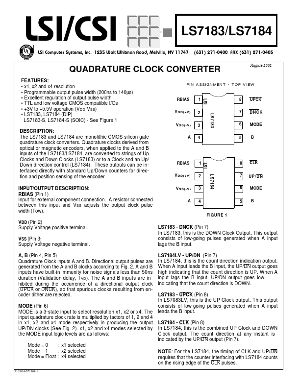
:● x1, x2 and x4 resolution
● Programmable output pulse width (200ns to 140µs)
● Excellent regulation of output pulse width
● TTL and low voltage CMOS compatible I/Os
● +3V to +5.5V operation (VDD-VSS)
● LS7183, LS7184 (DIP) LS7183-S, LS7184-S (SOIC) - See Figure 1
DESCRIPTION
: The LS7183 and LS7184 are monolithic CMOS silicon gate quadrature clock converters. Quadrature clocks derived from optical or magnetic encoders, when applied to the A and B inputs of the LS7183/LS7184, are converted to strings of Up Clocks and Down Clocks (LS7183) or to a Clock and an Up/ Down direction control (LS7184). These outputs can be interfaced directly with standard Up/Down counters for direction and position sensing of the encoder. INPUT/OUTPUTDESCRIPTION
: RBIAS (Pin 1) Input for external component connection. A resistor connected between this input and VSS adjusts the output clock pulse width (Tow). VDD (Pin 2) Supply Voltage positive terminal. VSS (Pin 3) Supply Voltage negative terminal. A, B (Pin 4, Pin 5) Quadrature Clock inputs A and B.