L9A0212
L9A0212 is Microprocessor manufactured by LSI.
Features ponents
- Caches
- - 16 Kbytes of two-way set-associative I-Cache 8 Kbytes of direct-mapped D-Cache
- R3000 MIPS CPU executes MIPS II and MIPS16 instructions 32-bit FBus, a fast demultiplexed multimaster bus, with built in control of:
- -
- RAM, EPROM, or similar simple devices DRAM and SDRAM General-purpose I/O
- -
Clock module with integrated PLL and programmable clock speeds
Technology
- LSI Logic G11 Technology
- - 0.18 µ Leff (0.25 µ drawn) 2.5 or 1.8 V operation
- -
Two 32-bit Timers Fast MDU
- 4/5 cycle multiply and accumulate (32-bit to 64-bit)
Performance and patibility
- -
- -
- 34/35 cycle divide BBCC with four writeback buffers included
Clock speed is 85 MHz at 2.5 V (85 MIPS peak and estimated 68 MIPS sustained) Low power mode allows LR4102 to use minimal power when idle patible with the full range of MIPS and third-party software development tools 16-bit and 32-bit code can be mixed arbitrarily with full support on a subroutine basis All instructions execute in one cycle except for Load and Store, Move To Coprocessor, and Move From Coprocessor, which execute in two cycles, and MDU instructions, which execute in several cycles
- MMU with 64-entry TLB RAM
- EJTAG Version 2.0.0:
- Nonintrusive debug
- - Real-time PC trace
- Hardware breakpoints Serial ICE-1 Port included for
- backward patibility with other Tiny RISC designs JTAG Boundary Scan On-Chip Memory (OCM), 1 Kbyte
- -
- 2
Tiny RISC LR4102 Microprocessor
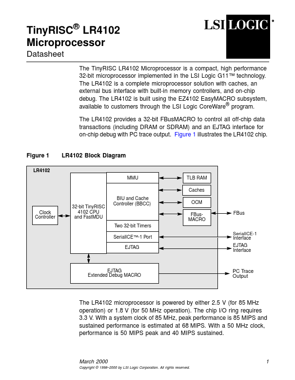
Block Diagram
This section provides short descriptions of the major ponents of the LR4102, as shown in Figure 1. The CPU...