GAL18V10
Overview
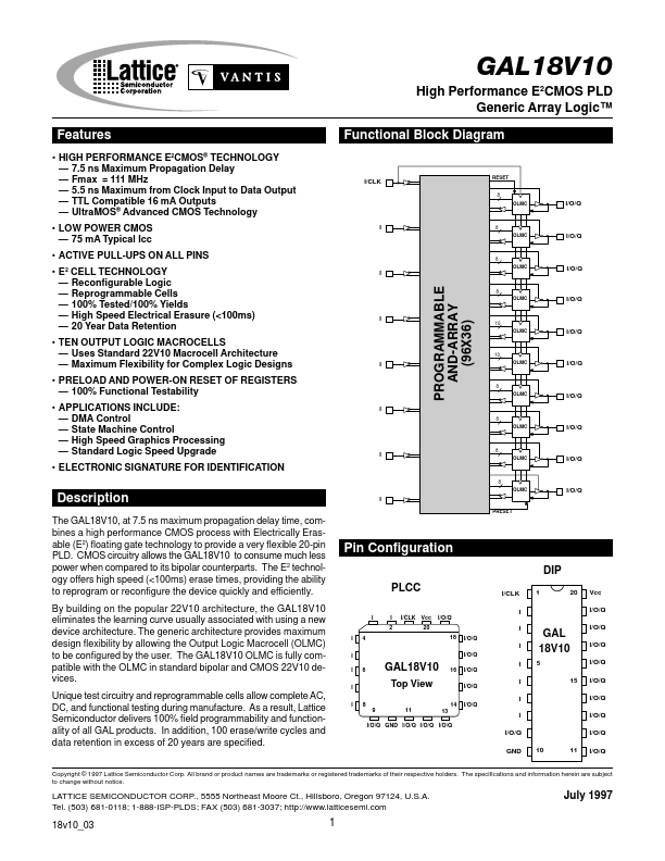
The GAL18V10, at 7.5 ns maximum propagation delay time, combines a high performance CMOS process with Electrically Erasable (E2) floating gate technology to provide a very flexible 20-pin PLD. CMOS circuitry allows the GAL18V10 to consume much less power when compared to its bipolar counterparts.
- HIGH PERFORMANCE E2CMOS® TECHNOLOGY - 7.5 ns Maximum Propagation Delay - Fmax = 111 MHz - 5.5 ns Maximum from Clock Input to Data Output - TTL Compatible 16 mA Outputs - UltraMOS® Advanced CMOS Technology
- LOW POWER CMOS - 75 mA Typical Icc
- ACTIVE PULL-UPS ON ALL PINS
- E2 CELL TECHNOLOGY - Reconfigurable Logic - Reprogrammable Cells - 100% Tested/100% Yields - High Speed Electrical Erasure (<100ms) - 20 Year Data Retention
- TEN OUTPUT LOGIC MACROCELLS - Uses Standard 22V10 Macrocell Architecture - Maximum Flexibility for Complex Logic Designs
- PRELOAD AND POWER-ON RESET OF REGISTERS - 100% Functional Testability