Lattice Semiconductor ISPCLOCK5500
In-System Programmable Zero-Delay
| Part No. | ISPCLOCK5500 |
|---|---|
| Datasheet | ISPCLOCK5500 Download |
| Manufacturer |  Lattice Semiconductor |
| Description | In-System Programmable Zero-Delay |
| Buy | Stock & Price |
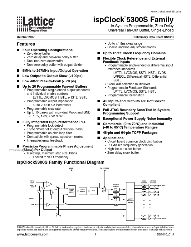
FEATURES
● Four Operating Configurations●
●
●
● Zero delay buffer Zero delay and non-zero delay buffer Dual non-zero delay buffer Non-zero delay buffer with output divider
● Up to +/- 5ns skew range
● Coarse and fine adjustment modes
● Up to Three Clock Frequency Domains
● Flexible Clock Reference and External Feedback Inputs
● Programmable single-ended or differential input reference standards - LVTTL, LVCMOS, SSTL, HSTL, LVDS, LVPECL, Differential HSTL, Differential SSTL
● Clock A/B selection multiplexer
● Programmable Feedback Standards - LVTTL, LVCMOS, SSTL, HSTL
● Programmable termination
● 8MHz to 267MHz Input/Output Operation
● Low Output to Output Skew (<100ps)
● Low Jitter Peak-to-Peak (< 70 ps)
● Up to 20 Programmable Fan-out Buffers
● Programmable single-ended output standards and individual enable controls - LVTTL, LVCMOS, HSTL, eHSTL, SSTL
● Programmable output impedance - 40 to 70Ω in 5Ω increments
● Programmable slew rate
● Up to 10 banks with individual VCCO and GND - 1.

