OR3T80
Overview
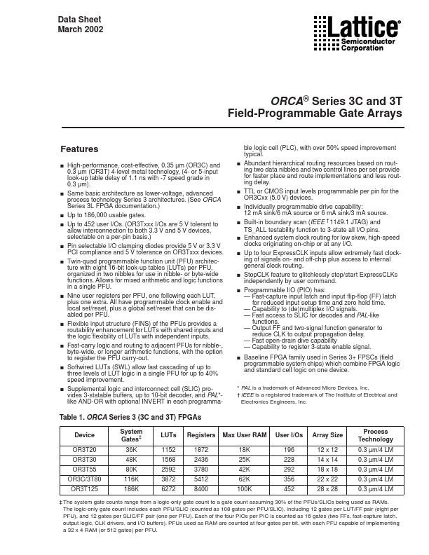
- High-performance, cost-effective, 0.35 µm (OR3C) and 0.3 µm (OR3T) 4-level metal technology, (4- or 5-input look-up table delay of 1.1 ns with -7 speed grade in 0.3 µm). Same basic architecture as lower-voltage, advanced process technology Series 3 architectures. (See ORCA Series 3L FPGA documentation.) Up to 186,000 usable gates. Up to 452 user I/Os. (OR3Txxx I/Os are 5 V tolerant to allow interconnection to both 3.3 V and 5 V devices, selectable on a per-pin basis.) Pin selectable I/O clamping diodes provide 5 V or 3.3 V PCI compliance and 5 V tolerance on OR3Txxx devices. Twin-quad programmable function unit (PFU) architecture with eight 16-bit look-up tables (LUTs) per PFU, organized in two nibbles for use in nibble- or byte-wide functions. Allows for mixed arithmetic and logic functions in a single PFU. Nine user registers per PFU, one following each LUT, plus one extra. All have programmable clock enable and local set/reset, plus a global set/reset that can be disabled per PFU. Flexible input structure (FINS) of the PFUs provides a routability enhancement for LUTs with shared inputs and the logic flexibility of LUTs with independent inputs. Fast-carry logic and routing to adjacent PFUs for nibble-, byte-wide, or longer arithmetic functions, with the option to register the PFU carry-out. Softwired LUTs (SWL) allow fast cascading of up to three levels of LUT logic in a single PFU for up to 40% speed improvement. Supplemental logic and interconnect cell (SLIC) provides 3-statable buffers, up to 10-bit decoder, and PAL*like AND-OR with optional INVERT in each programma- * * * * * * *
- ble logic cell (PLC), with over 50% speed improvement typical. Abundant hierarchical routing resources based on routing two data nibbles and two control lines per set provide for faster place and route implementatio