Datasheet4U Logo Datasheet4U.com

ispGDX160V-7Q208I Datasheet In-system Programmable 3.3v Generic Digital Crosspointtm

Manufacturer: Lattice Semiconductor

Datasheet Details

Part number ispGDX160V-7Q208I
Manufacturer Lattice Semiconductor
File Size 464.45 KB
Description In-System Programmable 3.3V Generic Digital CrosspointTM
Datasheet ispGDX160V-7Q208I_LatticeSemiconductor.pdf

ispGDX160V-7Q208I Overview

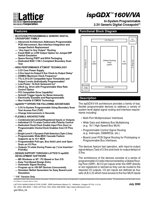
The ispGDXV/VA architecture provides a family of fast, flexible programmable devices to address a variety of system-level digital signal routing and interface requirements including: • Multi-Port Multiprocessor Interfaces • Wide Data and Address Bus Multiplexing (e.g. 16:1 High-Speed Bus MUX) • Programmable Control Signal Routing (e.g. Interrupts, DMAREQs, etc.) • Board-Level PCB Signal Routing for Prototyping or Programmable Bus Interfaces The devices feature fast operation, with input-to-output signal delays (Tpd) of 3.5ns and clock-to-output delays of 3.5ns. The architecture of the devices consists of a series of programmable I/O cells interconnected by a Global Routing Pool (GRP). All I/O pin inputs enter the GRP directly or are registered or latched so they can be routed to the required I/O outputs. I/O pin inputs are defined as four sets (A,B,C,D) which have access to the four MUX...

ispGDX160V-7Q208I Key Features

  • IN-SYSTEM PROGRAMMABLE GENERIC DIGITAL CROSSPOINT FAMILY
  • Advanced Architecture Addresses Programmable PCB Interconnect, Bus Interface Integration and Jumper/Switch Replacement
  • Fixed HIGH or LOW Output Option for Jumper/DIP Switch Emulation
  • Space-Saving PQFP and BGA Packaging
  • Dedicated IEEE 1149.1-pliant Boundary Scan Test
  • HIGH PERFORMANCE E2CMOS® TECHNOLOGY
  • 3.3V Core Power Supply
  • 3.5ns Input-to-Output/3.5ns Clock-to-Output Delay
  • 250MHz Maximum Clock Frequency

ispGDX160V-7Q208I Distributor