Lattice Semiconductor ispGDX80A-7T100
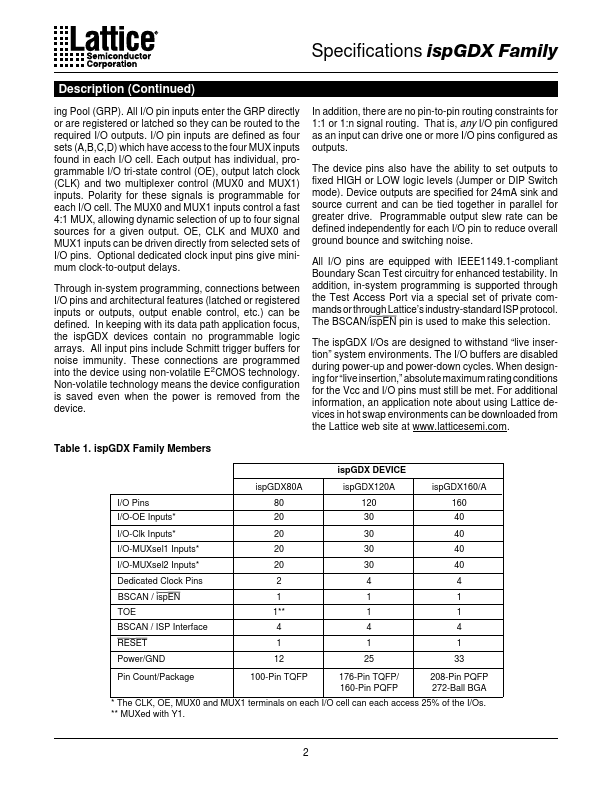
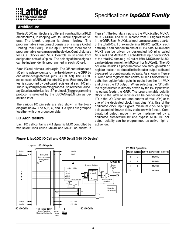
The ispGDX architecture provides a family of fast, flexible programmable devices to address a variety of systemlevel digital signal routing and interface requirements including: • Multi-Port Multiprocessor Interfaces • Wide Data and Address Bus Multiplexing (e.g. These devices are available in packages ranging from the 100-pin TQFP to the 208-pin PQFP. The devices feature fast operation, with input-to-output signal delays (Tpd) of 5ns and clockto-output delays of 5ns.| Part No. | ispGDX80A-7T100 |
|---|---|
| Datasheet | ispGDX80A-7T100 Download |
| Manufacturer |  Lattice Semiconductor |
| Description | In-System Programmable Generic Digital CrosspointTM |
| Buy | Stock & Price |

FEATURES
● IN-SYSTEM PROGRAMMABLE GENERIC DIGITAL CROSSPOINT FAMILY — Advanced Architecture Addresses Programmable PCB Interconnect, Bus Interface Integration and Jumper/Switch Replacement — Three Device Options: 80 to 160 Programmable I/O Pins — “Any Input to Any Output” Routing — Fixed HIGH or LOW Output Option for Jumper/DIP Switch Emulation — Space-Saving TQFP, PQFP and BGA Packaging — Dedicated IEEE 1149.1-Compliant Boundary Scan Test — PCI Compliant Output Drive● HIGH PERFORMANCE E2CMOS® TECHNOLOGY — 5V Power Supply — 5.0ns Input-to-Output/5.0ns Clock-to-Output Delay — Low-Power: 40mA Quiescent Icc — Balanced 24mA Output Buffers with Programmable Slew Rate Control — Schmitt Trigger Inputs for Noise Immunity — Electrically Erasable and Reprogrammable — Non-Volatile E2CMOS Technology — 100% Tested
● ispGDX OFFERS THE FOLLOWING ADVANTAGES — In-System Programmable — Lattice ISP or JTAG Programming Interface — Only 5V Power Supply Required — Change Interconnects in Seconds — Reprogra...