Lattice OR2C06A
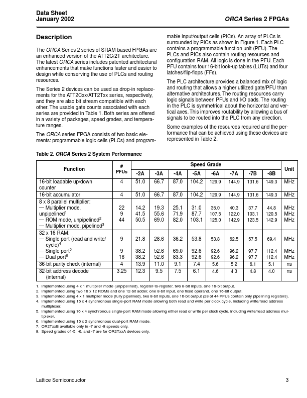
the OR2CxxA (5 V) devices Individually programmable drive capability: 12 mA sink/6 mA source or 6 mA sink/3 mA source Built-in boundary scan (IEEE *1149.1 JTAG) and 3-state all I/O pins, (TS_ALL) testability functions Multiple configuration options, including simple, low pincount serial ROMs, and peripheral or JTAG modes for insystem programming (ISP) Full PCI bus compliance for all devices Supported by industry-standard CAE tools for design entry, synthesis, and simulation with ORCA Foundry Development System support (for back-end implementation) New, added features (OR2TxxB) have: — More I/O... The second number assumes 30% of a design is RAM.
 Lattice