GENERAL DESCRIPTION
: It can be used in a wide variety of applications. FEATURES
: l Fast Switching l Low Gate Charge and RDS(ON) l Low Reverse transfer capacitances APPLICATIONS
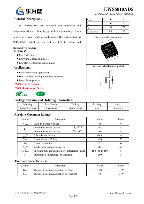
: l Battery switching application l Hard switched and high frequency circuits l Power Management 100% DVDS Tested 100% Avalanche Tested LWS6010AD5 LW Silicon P-Channel Power MOSFET VDSS ID PD RDS(ON) TYPE -60 V -60 A 104 W 9.0 mΩ Marking and Pin Assignment Inner Equivalent Principium Chart Package Marking and Ordering Information: Marking Part Number Package S6010/LW D5/D.C. LWS6010AD5 PDFN5*6-8L ABSOLUTE MAXIMUM RATINGS
: Symbol Parameter VDSS ID IDMa1 VGS PD EASa2 TJ, TSTG TL Drain-to-Source Voltage Continuous Drain Current Continuous Drain Current Pulsed Drain Current TC=25℃ TC=100℃ Gate-to-Source Voltage Power Dissipation Single pulse avalanche energy Operating Junction and Storage Temperature Range Maximum Temperature for Soldering Thermal Characteristics: Symbol Parameter RθJC Thermal Resistance, Junction-to-Case RθJA Thermal Resistance, Junction-to-Ambient Packing Reel Qty.