LTC1928-5
LTC1928-5 is Doubler Charge Pump manufactured by Linear Technology.
LTC1928-5 Doubler Charge Pump with Low Noise Linear Regulator in Thin SOT
Features s s s s s s s s s s s
DESCRIPTIO
U APPLICATIO S s s s s s s s s
Low Output Noise: 90µVRMS (100k Hz BW) Fixed Output Voltage: 5V Input Voltage Range: 2.7V to 4.4V No Inductors Required Uses Small Ceramic Capacitors Output Current Up to 30m A 550k Hz Switching Frequency Low Operating Current: 190µA Low Shutdown Current: 4µA Internal Thermal Shutdown and Current Limiting Low Profile (1mm) Thin SOTTM Package
The LTC®1928-5 is a doubler charge pump with an internal low noise, low dropout (LDO) linear regulator. The part is designed to provide a low noise boosted supply voltage for powering noise sensitive devices such as high frequency VCOs in wireless applications. An internal charge pump converts a 2.7V to 4.4V input to a boosted output, while the internal LDO regulator converts the boosted voltage to a low noise regulated output. The regulator is capable of supplying up to 30m A of output current. Shutdown reduces the supply current to < 8µA, removes the load from VIN by disabling the regulator and discharges VOUT to ground through a 200Ω switch. The LTC1928-5 LDO regulator is stable with only 2µF on the output. Small ceramic capacitors can be used, reducing PC board area. The LTC1928-5 is short-circuit and overtemperature protected. The part is available in a 6-pin low profile (1mm)Thin SOT package.
, LTC and LT are registered trademarks of Linear Technology Corporation Thin SOT is a trademark of Linear Technology Corporation.
VCO Power Supplies for Cellular Phones 2-Way Pagers Wireless PCMCIA Cards Portable Medical Instruments Low Power Data Acquisition Remote Transmitters White LED Drivers Ga As Switches
TYPICAL APPLICATION
LTC1928-5 VIN 2.7V TO 4.4V 1 4.7µF 0.47µF 5 6 VIN CP VOUT CPO 3 4 2 4.7µF
19285 F01
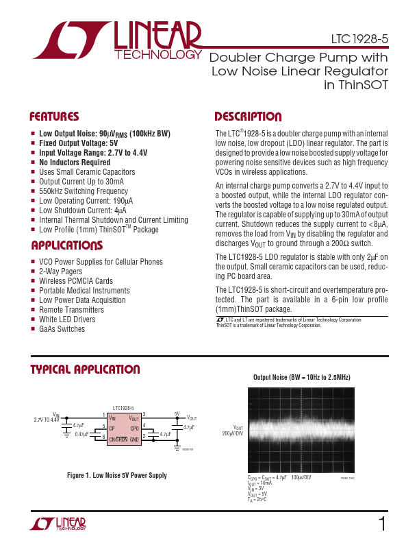
Output Noise (BW = 10Hz to 2.5MHz)
5V
VOUT 4.7µF VOUT 200µV/DIV
CN/SHDN GND
Figure 1. Low Noise 5V Power Supply
CCPO = COUT = 4.7µF 100µs/DIV IOUT = 10m A VIN = 3V VOUT = 5V...