LTC2281
LTC2281 is 125Msps Low Power 3V ADC manufactured by Linear Technology.
Features n Integrated Dual 10-Bit ADCs n Sample Rate: 125Msps n Single 3V Supply (2.85V to 3.4V) n Low Power: 790m W n 61.6d B SNR, 88d B SFDR n 110d B Channel Isolation at 100MHz n Flexible Input: 1VP-P to 2VP-P Range n 640MHz Full Power Bandwidth S/H n Clock Duty Cycle Stabilizer n Shutdown and Nap Modes n Data Ready Output Clock n Pin patible Family
125Msps: LTC2283 (12-Bit), LTC2281 (10-Bit) 105Msps: LTC2282 (12-Bit), LTC2280 (10-Bit) 80Msps: LTC2294 (12-Bit), LTC2289 (10-Bit) 65Msps: LTC2293 (12-Bit), LTC2288 (10-Bit) 40Msps: LTC2292 (12-Bit), LTC2287 (10-Bit) n 64-Pin (9mm × 9mm) QFN Package
APPLICATIONS n Wireless and Wired Broadband munication n Imaging Systems n Spectral Analysis n Portable Instrumentation
Dual 10-Bit, 125Msps Low Power 3V ADC
DESCRIPTION
The LTC®2281 is a 10-bit 125Msps, low power dual 3V A/D converter designed for digitizing high frequency, wide dynamic range signals. The LTC2281 is perfect for demanding imaging and munications applications with AC performance that includes 61.6d B SNR and 82d B SFDR for signals at the Nyquist frequency.
Typical DC specs include ±0.1LSB INL, ±0.1LSB DNL. The transition noise is a low 0.08LSBRMS.
A single 3V supply allows low power operation. A separate output supply allows the outputs to drive 0.5V to 3.6V logic.
A single-ended CLK input controls converter operation. An optional clock duty cycle stabilizer allows high performance at full speed for a wide range of clock duty cycles. A data ready output clock (CLKOUT) can be used to latch the output data.
L, LT, LTC and LTM are registered trademarks of Linear Technology Corporation. All other trademarks are the property of their respective owners.
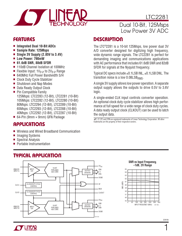
TYPICAL APPLICATION
ANALOG INPUT A
+
INPUT S/H
- 10-BIT PIPELINED ADC CORE
CLK A CLK B
CLOCK/DUTY CYCLE CONTROL
CLOCK/DUTY CYCLE CONTROL
ANALOG INPUT B
+
INPUT S/H
- 10-BIT PIPELINED ADC CORE
OUTPUT DRIVERS
OVDD D9A
- -
- D0A OGND
MUX CLKOUT
OUTPUT DRIVERS
OVDD D9B
-...