LTC3410-1.875 Overview
Key Features
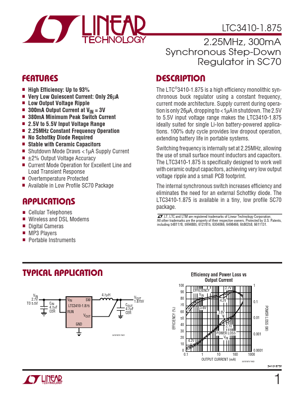
- High Efficiency: Up to 93%
- Very Low Quiescent Current: Only 26µA
- Low Output Voltage Ripple
- 300mA Output Current at VIN = 3V
- 380mA Minimum Peak Switch Current
| Part | LTC3410-1.875 |
|---|---|
| Description | 300mA Synchronous Step-Down Regulator |
| Category | Voltage Regulator |
| Manufacturer | Linear Technology |
| Size | 232.59 KB |
| Part Number | Manufacturer | Description |
|---|---|---|
| LM317 | Texas Instruments | 3-Terminal Adjustable Regulator |
| TL431 | Fairchild Semiconductor | Programmable Shunt Regulator |
| LM317 | Inchange Semiconductor | Adjustable Voltage Regulator |