Linear Technology LTC1150
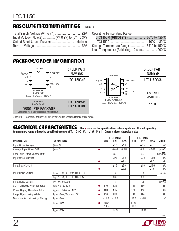
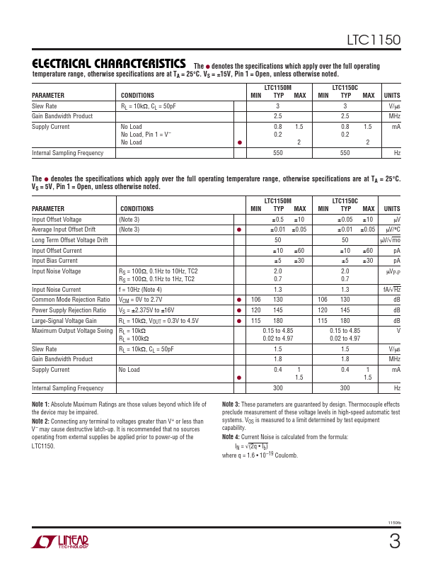
the LTC1150 to operate at up to 32V total supply voltage. The LTC1150 has an offset voltage of 0.5µV, drift of 0.01µV/°C, 0.1Hz to 10Hz input noise voltage of 1.8µVP-P and a typical voltage gain of 180dB. The slew rate of 3V/µs and a gain bandwidth product of 2.5MHz are achieved with 0.8mA of supply current.| Part No. | LTC1150 |
|---|---|
| Datasheet | LTC1150 Download |
| Manufacturer |  Linear Technology |
| Description | +-15V Chopper Stabilized Operational Amplifier |
| Buy | Stock & Price |
FEATURES
● High Voltage Operation: ±16V● No External Components Required
● Maximum Offset Voltage: 10µV
● Maximum Offset Voltage Drift: 0.05µV/°C
● Low Noise 1.8µVP-P (0.1Hz to 10Hz)
● Minimum Voltage Gain: 135dB
● Minimum PSRR: 120dB
● Minimum CMRR: 110dB
● Low Supply Current: 0.8mA
● Single Supply Operation: 4.75V to 32V
● Input Common Mode Range Includes Ground
● 200µA Supply Current with Pin 1 Grounded
● Typical Overload Recovery Time 20ms U APPLICATIO S
● Strain Gauge Amplifiers
● Electronic Scales
● Medical Instrumentation
● Thermocouple Amplifiers
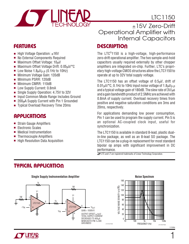
● High Resolution Data Acquisition LTC1150 ±15V Zero-Drift Operational Amplifier with Internal Capacitors DESCRIPTIO The LTC®1150 is a high-voltage, high-performance zero-drift operational amplifier. The two sample-and-hold capacitors usually required externally by other chopper amplifiers are integrated on-chip. Further, LTC’s proprietary high-voltage CMOS structures allow Overload recovery times from positive and negative saturation conditions are 3ms and 20ms, respectively.