FEATURES
s s DESCRIPTION
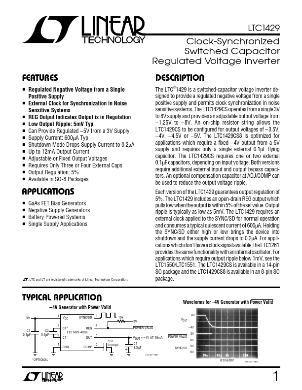
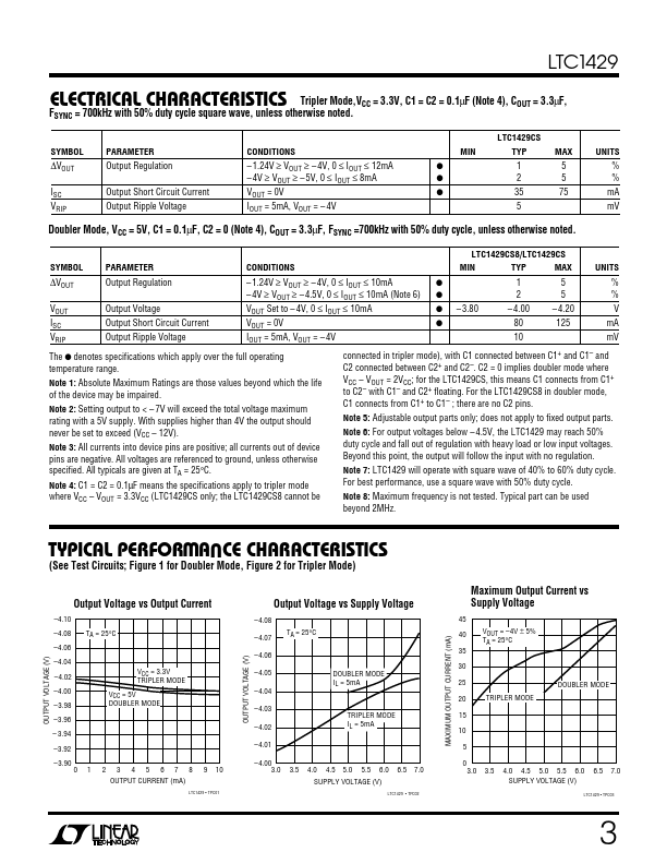
The LTC ®1429 is a switched-capacitor voltage inverter designed to provide a regulated negative voltage from a single positive supply and permits clock synchronization in noise sensitive systems. The LTC1429CS operates from a single 3V to 8V supply and provides an adjustable output voltage from – 1.25V to – 8V. An on-chip resistor string allows the LTC1429CS to be configured for output voltages of – 3.5V, –4V, –4.5V or – 5V. The LTC1429CS8 is optimized for applications which require a fixed –4V output from a 5V supply and requires only a single external 0.1µF flying capacitor. The LTC1429CS requires one or two external 0.1µF capacitors, depending on input voltage. Both versions require additional external input and output bypass capacitors. An optional compensation capacitor at ADJ/COMP can be used to reduce the output voltage ripple. Each version of the LTC1429 guarantees output regulation of 5%. Output ripple is typically as low as 5mV. Holding the SYNC/SD either high or low brings the device into shutdown and the supply current drops to 0.2µA. Linear Technology