FEATURES
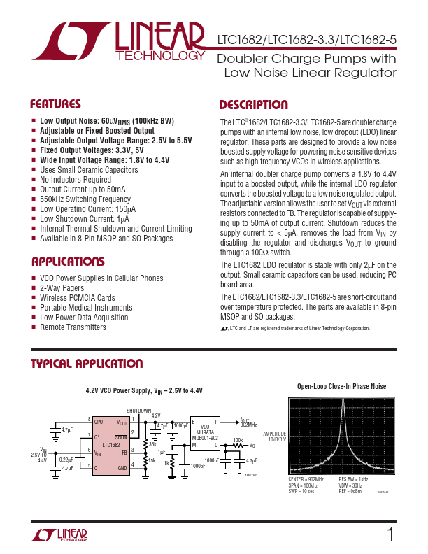
s s s s s s s s s s s s s DESCRIPTIO Low Output Noise: 60µVRMS (100kHz BW) Adjustable or Fixed Boosted Output Adjustable Output Voltage Range: 2.5V to 5.5V Fixed Output Voltages: 3.3V, 5V Wide Input Voltage Range: 1.8V to 4.4V Uses Small Ceramic Capacitors No Inductors Required Output Current up to 50mA 550kHz Switching Frequency Low Operating Current: 150µA Low Shutdown Current: 1µA Internal Thermal Shutdown and Current Limiting Available in 8-Pin MSOP and SO Packages U APPLICATIO S s s s s s s VCO Power Supplies in Cellular Phones 2-Way Pagers Wireless PCMCIA Cards Portable Medical Instruments Low Power Data Acquisition Remote Transmitters The LTC®1682/LTC1682-3.3/LTC1682-5 are doubler charge pumps with an internal low noise, low dropout (LDO) linear regulator. These parts are designed to provide a low noise boosted supply voltage for powering noise sensitive devices such as high frequency VCOs in wireless applications. An internal doubler charge pump converts a 1.8V to 4.4V input to a boosted output, while the internal LDO regulator converts the boosted voltage to a low noise regulated output. Linear Technology