FEATURES
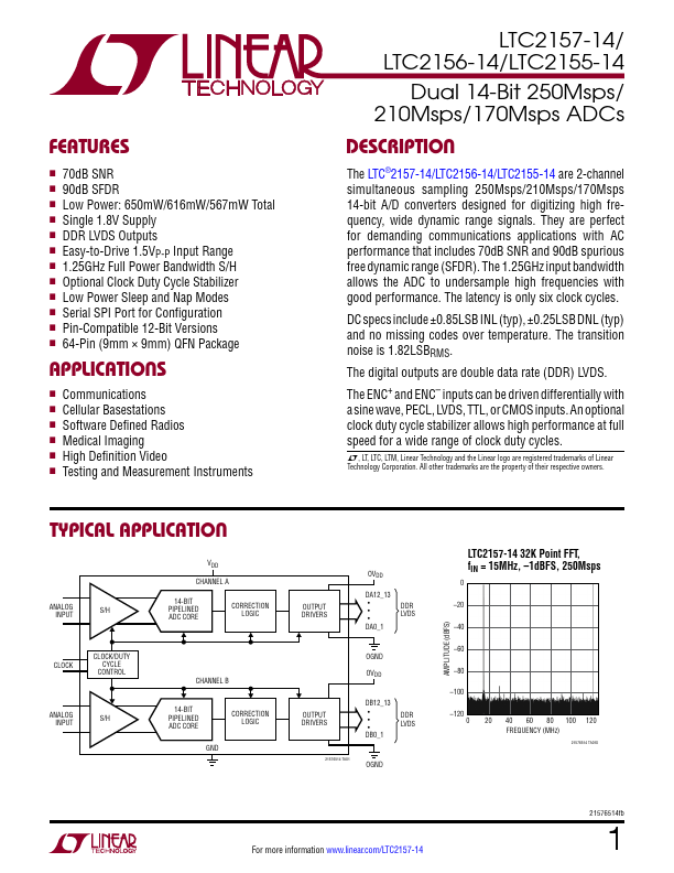
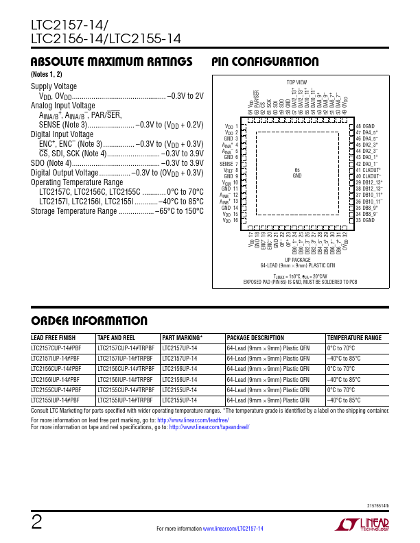
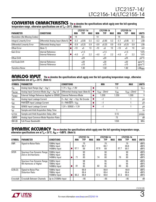
n 70dB SNR n 90dB SFDR n Low Power: 650mW/616mW/567mW Total n Single 1.8V Supply n DDR LVDS Outputs n Easy-to-Drive 1.5VP-P Input Range n 1.25GHz Full Power Bandwidth S/H n Optional Clock Duty Cycle Stabilizer n Low Power Sleep and Nap Modes n Serial SPI Port for Configuration n Pin-Compatible 12-Bit Versions n 64-Pin (9mm × 9mm) QFN Package APPLICATIONS
n Communications n Cellular Basestations n Software Defined Radios n Medical Imaging n High Definition Video n Testing and Measurement Instruments LTC2157-14/ LTC2156-14/LTC2155-14 Dual 14-Bit 250Msps/ 210Msps/170Msps ADCs DESCRIPTION
The 1.25GHz input bandwidth allows the ADC to undersample high frequencies with good performance. The latency is only six clock cycles. DC specs include ±0.85LSB INL (typ), ±0.25LSB DNL (typ) and no missing codes over temperature. The transition noise is 1.82LSBRMS. The digital outputs are double data rate (DDR) LVDS. The ENC+ and ENC– inputs can be driven differentially with a sine wave, PECL, LVDS, TTL, or CMOS inputs. Linear Technology